
Printed circuit boards (PCBs) are indispensable components in the architecture of modern electronics. Acting as the central nervous system of electronic devices, PCBs meticulously route electrical signals, enabling seamless communication and functionality among various electronic components. Without these intricate boards, the sophisticated devices we rely on daily would simply cease to function.
The demand for high-quality PCBs is intrinsically linked to the relentless advancement of technology. As consumers continually expect more sophisticated and compact electronics, the expertise of a reliable Printed Circuit Manufacturer becomes paramount. The global PCB market is robust and expanding, projected to reach a staggering $107.6 billion by 2030, driven by the burgeoning electronics industry and the proliferation of Internet of Things (IoT) devices. This growth underscores the critical role of proficient printed circuit manufacturers in supporting technological innovation and global connectivity.
Understanding the PCB Manufacturing Process
A printed circuit board is fundamentally a non-conductive substrate meticulously crafted with conductive pathways, known as traces. These traces, typically made of copper, are etched or printed onto the base material, forming the electrical circuitry. Electronic components are then strategically mounted and soldered onto the board, with the traces acting as the highways for electrical signals, creating a functional circuit. PCBs are the unsung heroes within most electronic devices, providing not only electrical connectivity but also crucial physical support and mechanical stability to the components they host.
The journey of industrial PCB manufacturing is a complex orchestration of numerous steps, rigorous quality checks, and precise adjustments. This meticulous process ensures that each finished PCB operates as intended, meeting stringent performance and reliability standards. While circuit boards can vary in complexity, ranging from single-layer to double-layer and intricate multilayer designs, the foundational manufacturing steps remain consistent up to the creation of the first conductive layer. The subsequent stages are tailored to the specific type and complexity of the PCB. Many advanced PCBs, especially those designed for high-performance applications, may require over 20 distinct manufacturing steps to achieve the desired functionality and quality.
Exploring Different Types of Printed Circuit Board Designs
The landscape of PCB design is diverse, with classifications based on design specifications, manufacturing methodologies, and intended applications. A skilled printed circuit manufacturer should be adept at producing a wide array of PCB types, including:
Single-Sided PCBs
Single-sided PCBs are the most basic and widely used type, featuring a conductive copper layer on one side of the substrate. Electronic components are mounted on this same side, while the etched circuit pattern is visible on the reverse. Due to their single conductive layer, trace pathways cannot intersect, which can limit design density.
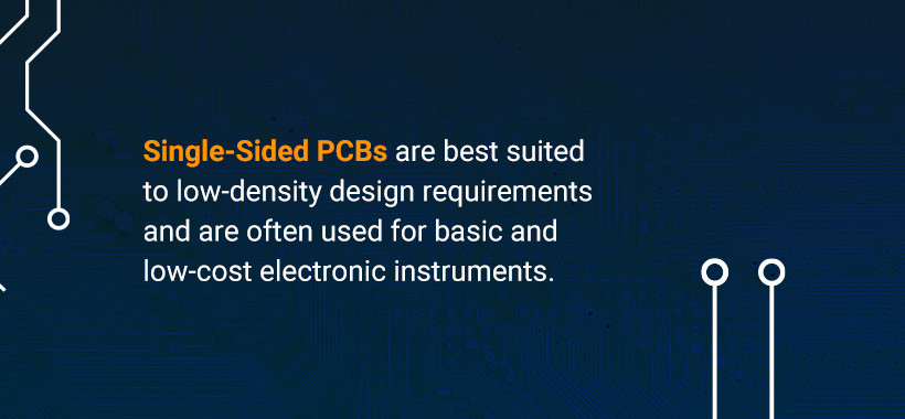 Single-Sided PCBs are best suited to low-density design requirements and are often used for basic and low-cost electronic instruments.
These PCBs are optimally suited for applications with lower design density requirements, commonly found in simple and cost-sensitive electronic devices. Their straightforward design translates to cost-effectiveness and relative ease of design, manufacturing, and repair, making them a practical choice for numerous basic electronic instruments.
Double-Sided PCBs
Double-sided PCBs represent a step up in complexity, featuring conductive layers on both the top and bottom sides of the board. Connectivity between these layers is achieved through drilled holes, allowing traces and component pins to establish circuits on both sides. Printed circuit manufacturers utilize various plating and via techniques to create these inter-layer connections.
This design offers significant advantages, including a more compact footprint for denser circuits, enhanced cost-efficiency compared to multilayer PCBs, and increased circuit density. These benefits render double-sided PCBs suitable for more advanced electronic systems where space and performance are key considerations.
Multilayered PCBs
Multilayered PCBs are at the high end of PCB complexity, incorporating more than two copper layers. They are constructed akin to a sandwich, with multiple conductive layers separated by insulating prepreg material. These layers are meticulously bonded and laminated together under intense pressure and heat to eliminate any air gaps and ensure the structural integrity of the PCB assembly. A proficient printed circuit manufacturer must have specialized equipment and expertise to produce high-quality multilayer PCBs.
Multilayer PCBs are essential for high-speed and high-density circuits due to their compactness and superior design flexibility. Their complex structure allows for intricate routing and signal management, making them indispensable in sophisticated electronic devices and high-performance applications.
Rigid PCBs
Rigid PCBs are characterized by their solid, inflexible substrate material, which provides the board with significant rigidity and strength, preventing bending or flexing. They can be single-sided, double-sided, or multilayered, and typically consist of several layers bonded together:
- Substrate: The foundation of the PCB, providing structural integrity.
- Copper Layers: Conductive layers for circuit traces.
- Solder Mask: A protective layer preventing solder bridging and environmental damage.
- Silkscreen: Printed ink layer for component placement guidance and identification.
These layers are fused together using a combination of adhesive and heat. Rigid PCBs are known for their durability and ease of maintenance, making them ideal for applications ranging from medical equipment to computer motherboards, where reliability and robustness are critical.
Flex PCBs
Flex PCBs are constructed using flexible substrates like polyamide, PEEK, or transparent conductive polyester films, allowing the circuit board to bend and conform to various shapes. They can be single-sided, double-sided, or multilayered, offering versatility in design and application. A specialized printed circuit manufacturer is needed for flex PCBs due to the unique material handling and processing requirements.
Beyond their flexibility, these PCBs are compact, highly reliable, and offer excellent signal integrity, making them ideal for applications requiring high signal trace density and flexibility, such as in automotive electronics, wearable technology, and mobile devices.
A Brief History of PCB Fabrication
The concept of the printed circuit board dates back to the early 20th century, with German inventor Albert Hansen filing the first patent for a rudimentary PCB in 1903. However, it was the latter half of the 20th century that witnessed significant advancements in PCB technology. The past 50 years have seen exponential growth in PCB functionality and miniaturization, enabling increasingly powerful electronics in smaller form factors.
The military played a pivotal role in advancing PCB production techniques during and after World War II. The U.S. Army Signal Corps pioneered methods to accelerate PCB production through automated assembly, making mass production more efficient and economically viable for consumer electronics. This innovation was crucial in transitioning PCBs from niche military applications to widespread use in commercial products.
The continuous evolution over the last half-century has led to the sophisticated, lightweight, and highly functional PCBs we see today. These advancements are paving the way for new technological frontiers, from autonomous vehicles to smart homes, where PCBs will continue to be the enabling technology. A forward-thinking printed circuit manufacturer stays abreast of these historical developments and continuously innovates to meet future demands.
Key Components of a PCB
Understanding the fundamental parts of a PCB is essential for appreciating the manufacturing process. A typical PCB comprises four primary components:
- Substrate: Often made of fiberglass (FR-4 is common), the substrate provides the structural base and rigidity to the PCB. It is considered by many to be the most crucial component, acting as the skeleton that provides strength and stability under mechanical stress.
- Copper Layer: This conductive layer, made of copper foil or coating, forms the circuit traces. It functions similarly to the nervous system, carrying electrical signals throughout the PCB, connecting components and enabling circuit operation.
- Solder Mask: A protective polymer layer applied over the copper layer, the solder mask acts as the PCB’s skin. It prevents copper oxidation, protects traces from damage, and confines solder to designated areas during component assembly, preventing short circuits. It is important to note that the solder mask is not designed to be a dielectric.
- Silkscreen: Also known as the legend or nomenclature, the silkscreen is typically printed on the component side of the PCB. It provides vital information such as component part numbers, symbols, switch settings, test points, and component reference designators, aiding in assembly, testing, and servicing.
The Intricate Process: How PCBs are Made, Step-by-Step
The creation of a PCB is a multi-stage process, commencing with design and verification and culminating in the fabrication of the physical circuit boards. Precision is paramount at each stage, often requiring computer-aided design (CAD) and machine-driven tools to ensure accuracy and minimize defects like short circuits or open circuits. Before leaving the printed circuit manufacturer, completed PCBs undergo rigorous testing to guarantee performance and reliability.
Step One: PCB Design – The Blueprint
 Design is the first step in PCB manufacturing. It acts as a plan for PCB manufacture and design — the designer lays out a blueprint for the PCB that fulfills all the outlined requirements.
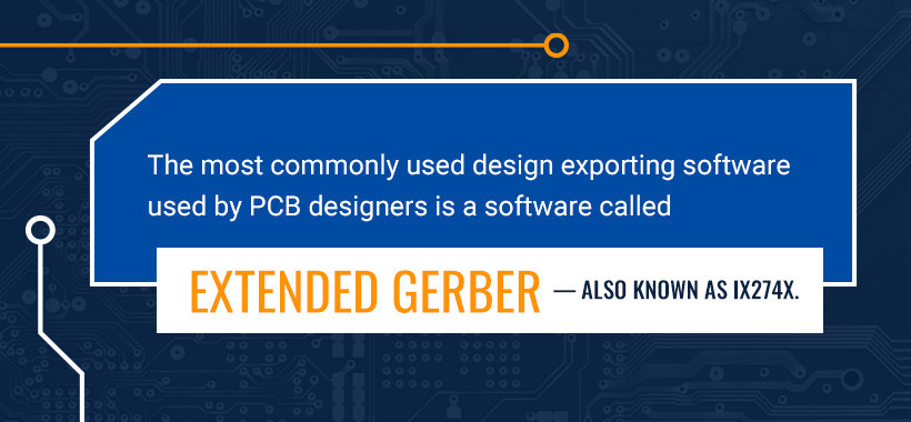
The PCB manufacturing journey begins with design. This crucial initial step involves creating a comprehensive blueprint that dictates every aspect of the PCB’s fabrication. Designers utilize specialized software, with Extended Gerber (also known as IX274X) being a widely adopted standard in the industry.
Extended Gerber software excels as a PCB design solution due to its robust output format. It generates all essential manufacturing data, including the number of copper layers, solder masks, component notations, and drill files. This comprehensive digital package ensures that both designers and printed circuit manufacturers have a unified understanding of the PCB specifications.
Once the design blueprint is finalized in Extended Gerber format, it undergoes thorough internal checks to identify and rectify any potential errors. Upon designer verification, the design files are transmitted to a PCB fabrication house. Here, fabricators conduct a Design for Manufacture (DFM) check. An effective DFM analysis is critical to confirm that the design is manufacturable within the fabricator’s process capabilities and will not incur excessive time or resource consumption.
Progressive engineering practices advocate for involving the printed circuit manufacturer in a DFM review during the design phase itself. This proactive approach allows for early identification and resolution of manufacturability issues, potentially saving both time and costs. Omissions or critical attribute oversights in the design can significantly impede the manufacturer’s ability to produce PCBs with high yield and quality.
Step Two: Design Review and Engineering Queries – Ensuring Accuracy
A critical checkpoint in the PCB fabrication process is the design review stage. This step involves a meticulous examination of the PCB design to identify any potential errors, design flaws, or manufacturability concerns. Experienced engineers scrutinize every facet of the design, ensuring no components are missing, and all structures are correctly defined.
Only upon receiving clearance from both the engineering review and client approval does the design proceed to the printing phase. Client approval often includes verification of all working files, array construction, tooling holes, multi-up array orientation, scoring, and snap-tab specifications, ensuring alignment with project requirements and manufacturability considerations.
Step Three: Printing – Transferring the Design to Film
PCB fabrication employs a specialized printing process distinct from conventional document printing. It requires a high-precision plotter printer to generate a PCB film, which serves as a photo negative of the PCB design.
For inner layers, the plotter printer uses two contrasting ink colors:
- Black ink: Represents the conductive circuits and copper traces of the PCB.
- Clear ink: Denotes the non-conductive areas, such as the fiberglass substrate.
This color scheme is reversed for the outer layers. Clear ink outlines the copper pathways, while black ink indicates areas where copper will be removed during subsequent processing.
Each PCB layer and its corresponding solder mask requires a separate film. Consequently, a simple two-layer PCB necessitates four film sheets – one for each layer and one for each solder mask.
After printing, all films for each layer are meticulously aligned, and a punch machine creates registration holes through all sheets. These registration holes act as alignment guides, ensuring accurate layer alignment throughout the subsequent manufacturing steps.
Step Four: Copper Printing for Inner Layers – Defining the Circuitry
In this step, the physical construction of the PCB begins. A laminate panel, the base material for the PCB, is coated with a photo-sensitive film known as resist. This resist is composed of photo-reactive chemicals that harden upon exposure to ultraviolet (UV) light. The resist facilitates precise transfer of the blueprint image onto the laminate.
The printed film, now acting as a stencil, is carefully aligned with the resist-coated laminate using the previously created registration holes. The assembly is then exposed to intense UV light.
UV light passes through the translucent areas of the film, hardening the photoresist underneath. These hardened areas correspond to the intended copper traces and conductive pathways. Conversely, the black ink on the film blocks UV light, preventing the resist in those areas from hardening. This differentiation is crucial for the subsequent copper etching process.
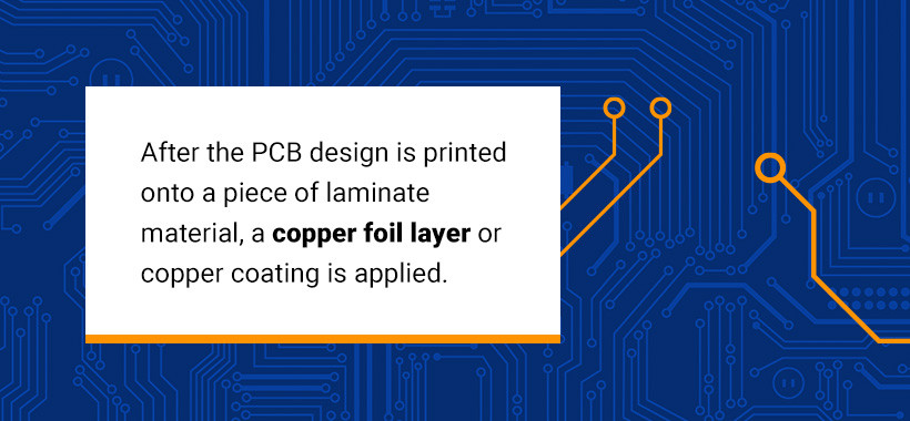 After the PCB design is printed onto a piece of laminate material, a copper foil layer or copper coating is applied.
Prior to resist application and imaging, a copper foil layer or copper coating is already bonded to the laminate material. This copper layer serves as the raw material from which the circuit traces will be formed. The subsequent etching process will selectively remove copper, leaving behind the designed circuit patterns.
The inner layers are typically part of a core, which is a pre-fabricated structure consisting of two copper layers separated by a dielectric material. Before etching, the inner layers are treated with an etch resist. This protective layer shields the copper intended to remain as traces from the etching chemicals. After etching, only the copper intended by the design remains, forming the conductive pathways.
Following etching, the board undergoes a cleaning process. Technicians use an alkaline solution or similar method to remove any residual photoresist from the non-trace areas. A pressure wash then removes any debris or particles from the surface, followed by drying. After drying, the only remaining resist should be on top of the copper traces. A meticulous inspection is then performed to identify any errors in the etched copper patterns.
Step Five: Etching Inner Layers – Copper Removal
To refine the inner layers or core of the PCB, excess copper must be removed. This is achieved through a chemical etching process. Etching involves selectively protecting the desired copper traces and exposing the rest of the copper surface to a chemical etchant. The etchant dissolves and removes the unprotected copper, precisely defining the circuit traces as per the design.
The duration of etching and the concentration of the copper etching solvent may vary depending on factors like PCB size and copper thickness. Larger PCBs or those with thicker copper layers may require longer etching times or stronger etchants to ensure complete removal of unwanted copper.
Step Six: Layer Alignment – Precise Positioning
After cleaning each inner layer, they are ready for precise layer alignment and optical inspection. The registration holes created in Step Three are now crucial for aligning the inner and outer layers accurately.
To achieve this alignment, technicians use an optical punch machine. This machine uses a pin that precisely aligns with the registration holes, ensuring each layer is perfectly positioned relative to the others. Accurate layer alignment is critical for the proper functioning of multilayer PCBs.
Step Seven: Automated Optical Inspection (AOI) – Quality Assurance
Following layer alignment, an Automated Optical Inspection (AOI) machine performs a critical quality check to detect any defects in the inner layers. AOI is paramount because once the layers are laminated together, any internal defects become irreparable.
The AOI system compares the manufactured PCB layer against the original Extended Gerber design data, acting as a digital reference. Any discrepancies, such as breaks in traces, shorts, or missing features, are flagged for review.
Successful completion of AOI, without detecting any defects, is essential for the PCB to proceed to the subsequent manufacturing stages. AOI serves as a critical mid-process quality checkpoint, preventing defective boards from progressing further and saving resources. This process is repeated for the outer layers after they undergo imaging and etching.
Step Eight: Lamination – Bonding the Layers
In this step, the pre-processed inner layers are combined with outer copper foil layers and insulating material to form the multilayer PCB structure. A dielectric material, typically prepreg (pre-impregnated epoxy resin), is placed between the inner core and the outer copper layers.
These layers are assembled in a specific stack-up sequence, often referred to as a “book,” and then placed in a specialized press table. Metal clamps and registration pins ensure precise layer alignment during the lamination process. A typical four-layer stack-up might consist of: copper foil, dielectric (prepreg), core (inner layers), dielectric (prepreg), and copper foil.
Once the stack-up is assembled and secured, it is transferred to a mechanical press. The press applies controlled pressure and heat to the stack. The heat melts the epoxy resin within the prepreg material, while the pressure compresses the layers together, effectively bonding and fusing the entire PCB stack into a cohesive multilayer structure. This lamination process creates a robust and electrically insulated PCB.
After lamination, the PCB stack is carefully removed from the press. The top press plate and registration pins are removed, allowing the now-laminated PCB panel to be extracted.
Step Nine: Drilling – Creating Component Holes and Vias
Before drilling, an X-ray drill is used to accurately locate the pre-determined drill positions on the PCB panel. Registration or guiding holes are drilled first to secure the PCB stack in the drilling machine and ensure precise alignment for subsequent drilling operations.
The actual component holes and vias (vertical interconnect access) are then drilled using a computer-numerical-controlled (CNC) drilling machine. This machine is programmed with the drill data extracted from the Extended Gerber design files, ensuring accurate hole placement and size.
After drilling, any excess copper burrs or debris along the edges of the holes are removed through a deburring process, ensuring clean and smooth holes for plating and component insertion.
Step Ten: PCB Plating – Establishing Electrical Connections
 After the panel has been drilled, it’s ready to be plated. The plating process uses a chemical to fuse all of the different layers of the PCB together.
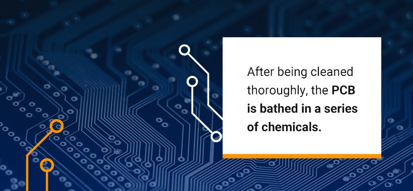
Following drilling, the PCB panel is prepared for plating. The plating process is crucial for establishing electrical connections between layers in multilayer PCBs and for creating conductive surfaces for component soldering.
The panel undergoes a thorough cleaning process to remove any contaminants. It is then immersed in a series of chemical baths. This chemical process deposits a thin layer of copper, typically micron-thick, over the entire panel surface, including the walls of the drilled holes. This process, known as electroless copper plating, creates a conductive layer throughout the holes, forming vias that connect different layers of the PCB.
Before copper plating, the drilled holes expose the non-conductive substrate material. Copper plating the hole walls effectively makes them conductive, enabling vertical electrical connections between layers.
Subsequently, the panel may undergo pattern plating, where a thicker layer of copper is selectively plated onto the traces and pads, enhancing conductivity and solderability. This step often involves applying another layer of resist and imaging to define the areas for thicker copper plating.
Step Eleven: Outer Layer Imaging – Defining External Circuitry
Similar to Step Four for inner layers, Step Eleven involves imaging the outer layers. A photoresist is applied to the outer copper layers of the PCB panel. Using a film plotter and UV light exposure, the circuit pattern for the outer layers is transferred onto the photoresist.
The photoresist hardens in areas exposed to UV light, corresponding to the desired copper traces and pads on the outer layers. The unhardened resist is then removed, leaving a patterned resist layer that will act as a mask during the subsequent etching process.
After imaging, the outer layers undergo plating, similar to the inner layers in Step Ten. However, for outer layers, a tin plating layer is often applied over the copper plating. This tin layer serves as an etch resist and solderability preservative for the copper traces on the outer layers.
Step Twelve: Outer Layer Etching – Final Copper Patterning
In the final etching stage, the tin plating acts as a protective layer, shielding the copper traces beneath it. The PCB panel is immersed in a copper etchant solution, which removes the unwanted copper from the outer layers – areas not protected by the tin plating.
This etching process precisely defines the final copper trace patterns on the outer layers, completing the circuit definition. After etching, the tin plating layer is removed using a chemical stripping process, revealing the finished copper circuitry of the outer layers.
The etching process for outer layers is considered a subtractive process, as it removes unwanted copper to create the desired circuit patterns, contrasting with additive processes that deposit conductive material to form traces.
Step Thirteen: Outer Layer AOI – Final Quality Verification
Similar to the inner layers, the outer layers undergo Automated Optical Inspection (AOI). This crucial quality control step ensures that the etched outer layer circuitry meets the design specifications and is free from defects.
The AOI machine compares the etched copper patterns on the outer layers to the original Gerber design data. It verifies that all unwanted copper has been removed, and the remaining copper traces and pads are correctly formed and positioned. AOI detects potential defects such as open circuits, short circuits, and trace width violations, ensuring the electrical integrity of the outer layers.
Passing AOI for the outer layers is a critical milestone in PCB fabrication, confirming the quality and functionality of the etched circuitry before proceeding to the final processing steps.
Step Fourteen: Solder Mask Application – Protection and Solderability
 Panels require a thorough cleaning before the solder mask is applied.
Before solder mask application, the PCB panels undergo a thorough cleaning process to ensure proper adhesion of the solder mask material. The solder mask, typically a liquid epoxy, is then applied to both sides of the PCB panel using methods like screen printing or curtain coating. After application, the solder mask is partially cured (tack-cured).
A visual inspection is performed to check for any solder mask defects, such as voids, inconsistencies, or misalignments. This inspection is critical, as many Original Equipment Manufacturers (OEMs) have stringent requirements and may not allow solder mask repairs. If defects are found, the solder mask may need to be stripped and reapplied.
If the solder mask passes visual inspection, it is fully cured through baking, hardening the epoxy and creating a durable protective layer. The solder mask protects the copper circuitry from environmental corrosion, oxidation, and physical damage. It also defines the solderable areas on the PCB, ensuring solder is confined to component pads during assembly and preventing solder bridges between traces.
For defining solder mask openings over component pads, a process called “liquid photo-imageable” (LPI) solder mask application is often used. UV light is selectively exposed through a photomask to define the areas where solder mask needs to be removed, creating openings for component soldering.
Step Fifteen: Silkscreen Application and Surface Finish – Final Touches
Silkscreen application, also known as legend or nomenclature printing, is the process of printing essential information onto the PCB surface. This information is crucial for assembly, testing, and servicing, and typically includes:
- Company identification numbers or logos
- Warning symbols
- Manufacturer’s marks
- Component part numbers and reference designators
- Pin locators and polarity markings
- Connector pin-outs
This information is typically printed using inkjet printers or screen printing techniques, often in white or yellow ink for contrast against the solder mask color. For fine-pitch components and small text sizes (8-point font or smaller), laser direct imaging may be used for higher precision silkscreen printing.
After silkscreen printing, the PCB surface finish is applied. The surface finish is a metallic coating applied to the exposed copper pads to protect them from oxidation and enhance solderability. The choice of surface finish depends on application requirements, cost considerations, and environmental compliance.
Step Sixteen: PCB Surface Finishes – Enhancing Performance and Protection
Finishing the PCB involves plating the exposed copper pads with conductive materials to provide a solderable and corrosion-resistant surface. Common PCB surface finishes include:
- Immersion Silver (ImAg): Offers excellent solderability and low signal loss, RoHS compliant and lead-free. However, it can tarnish and oxidize over time.
- Hard Gold: Highly durable and reliable, often used for edge connectors (gold fingers) requiring repeated insertions. Expensive but RoHS compliant and lead-free.
- Electroless Nickel Immersion Gold (ENIG): A popular and reliable finish offering good solderability, flatness, and corrosion resistance. More expensive than HASL but less than hard gold. RoHS compliant.
- Hot Air Solder Leveling (HASL): A cost-effective and robust finish with good reworkability. Contains lead and is not RoHS compliant.
- Lead-Free HASL: RoHS compliant version of HASL, offering similar cost and reworkability benefits without lead.
- Immersion Tin (ImSn): Suitable for press-fit applications and offers good planarity. Can have soldering issues like tin whiskers and a limited shelf life. RoHS compliant.
- Organic Solderability Preservative (OSP): A cost-effective, RoHS compliant organic coating that protects copper pads and provides good solderability. Limited shelf life.
- Electroless Nickel Electroless Palladium Immersion Gold (ENEPIG): A more complex and expensive finish offering excellent solderability, wire bonding capability, and corrosion resistance. Palladium layer prevents nickel corrosion.
The selection of the appropriate surface finish is crucial and depends on factors such as application environment, soldering requirements, component type, and cost constraints. A knowledgeable printed circuit manufacturer can advise on the best surface finish for specific needs.
Step Seventeen: Electrical Reliability Testing – Ensuring Functionality
After surface finishing, PCBs undergo rigorous electrical testing to verify their functionality and reliability. Electrical testing is typically performed according to IPC-9252 standards, “Guidelines and Requirements for Electrical Testing of Unpopulated Printed Boards.”
The primary electrical tests are:
- Circuit Continuity Test: Checks for open circuits (breaks in traces) by verifying that electrical current can flow through all intended conductive paths.
- Circuit Isolation Test: Verifies the insulation resistance between different conductive layers and traces, checking for short circuits (unintended electrical connections).
 While the electrical tests mainly exist to ensure functionality, they also work as a test of how well the initial PCB design stood up to the manufacturing process.
Beyond basic continuity and isolation tests, more advanced testing methods like “bed of nails” testing can be employed. In bed of nails testing, spring-loaded probes make contact with numerous test points on the PCB simultaneously, applying pressure to simulate component mounting and further assess electrical performance under stress.
Electrical testing serves as a final validation of the PCB design and manufacturing process, ensuring that only functional and reliable boards proceed to the next stages of assembly and deployment.
Step Eighteen: Profiling and Route Out – Separating Individual PCBs
Profiling, or route out, is the process of separating individual PCBs from the larger manufacturing panel. Fabrication engineers use the shape and size information from the Gerber design files to define the outline of each PCB.
Routing out involves using a CNC router or laser cutter to create scores or cut lines along the PCB outlines on the manufacturing panel. These scores weaken the panel along the PCB boundaries, allowing for easy separation of individual PCBs. Alternatively, V-groove scoring can be used, creating V-shaped cuts along the PCB outlines.
For high-volume production, a hard-tooled punch may be used to stamp out individual PCBs from the panel. In some cases, PCBs are designed with snap-tabs within the array, allowing for manual separation of individual boards after component assembly.
Step Nineteen: Final Quality Check and Visual Inspection – Last Line of Defense
Before packaging and shipping, each separated PCB undergoes a final comprehensive quality check and visual inspection. This inspection verifies various critical aspects:
- Hole Positioning and Tolerances: Hole sizes and positions must be accurate across all layers and meet design specifications.
- Board Dimensions: PCB dimensions must conform to the original design blueprints.
- Cleanliness: PCBs must be free from dust, debris, and processing residues.
- Finish Quality: PCB edges should be smooth, without burrs or sharp points. Surface finishes should be uniform and defect-free.
- Electrical Reliability: Any PCBs that failed electrical testing are re-inspected and re-tested after rework or rejection.
This final inspection acts as the last line of defense, ensuring that only PCBs meeting the highest quality standards are packaged and shipped to customers.
Step Twenty: Packaging and Delivery – Protecting and Shipping
The final stage of PCB manufacturing is packaging and delivery. PCBs are typically vacuum-sealed in moisture-barrier bags to protect them from humidity, dust, and contaminants during storage and transport.
The sealed PCBs are then placed in protective containers, such as cardboard boxes with cushioning material, to prevent physical damage during shipping. Depending on customer specifications and component sensitivity, electrostatic discharge (ESD) protective packaging may be used to safeguard against static electricity damage.
Finally, the packaged PCBs are shipped to the customer, completing the PCB manufacturing cycle.
Multilayer PCB Manufacturing: Additional Steps
Multilayer PCB fabrication incorporates additional steps to accommodate the increased complexity of multiple copper layers and cores. These additional steps are primarily focused on ensuring proper bonding and lamination of the multiple layers.
Inner Layer Imaging and Etching for Multilayers
The inner layer imaging and etching processes for multilayer PCBs are similar to those described in Steps Three, Four, and Five for single and double-sided PCBs. However, in multilayer fabrication, these steps are repeated for each inner layer.
For each inner layer, the design is printed onto film, transferred to a resist-coated laminate, and then etched to define the copper circuitry. Registration holes are crucial for aligning multiple inner layers accurately.
Resist Stripping and Post Etch Punch for Multilayers
 The resist stripping step removes any remaining resist covering the copper of the PCB inner layer.
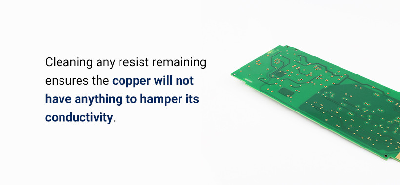
Following etching of each inner layer, resist stripping is performed to remove any remaining photoresist from the copper traces. This ensures clean copper surfaces for subsequent lamination.
Post-etch punching, using registration holes as guides, is repeated for each inner layer to maintain accurate layer alignment throughout the multilayer fabrication process.
Inner Layer AOI and Oxide Treatment for Multilayers
Automated Optical Inspection (AOI) is conducted for each inner layer to ensure quality and detect any defects before lamination.
Before lamination, inner layers undergo an oxide treatment. This chemical process creates a micro-roughened surface on the copper layers, enhancing the adhesion of the insulating prepreg material during the lamination process and improving inter-layer bonding strength.
Layup and Lamination for Multilayers
The layup and lamination steps for multilayer PCBs are more complex than for single or double-sided boards. Multiple layers of prepreg and inner layers are stacked together in a precise sequence, forming the multilayer stack-up.
The layup process is often automated, using robotic equipment to ensure accurate layer placement and alignment. Registration pins and tooling holes are critical for maintaining layer registration during layup and lamination.
Lamination of multilayer PCBs requires higher temperatures and pressures compared to simpler PCBs. This ensures proper melting and flow of the prepreg resin, filling all gaps and creating a void-free and robust multilayer structure. The lamination process is carefully controlled to achieve optimal bonding and electrical insulation between layers.
X-Ray Alignment and Drilling for Multilayers
When drilling multilayer PCBs, X-ray alignment is used to precisely locate the drill positions relative to the internal layers. This is crucial for accurate registration of drilled holes with inner layer circuitry, especially for vias that connect multiple layers.
X-ray alignment ensures that drilled holes are accurately positioned through all layers of the multilayer PCB, enabling reliable inter-layer connections. After X-ray alignment, drilling is performed, followed by the standard PCB plating and subsequent manufacturing steps.
Implementing Effective PCB Manufacturing Processes
Effective PCB manufacturing hinges on seamless collaboration and clear communication between design entities (OEMs) and printed circuit manufacturers (CMs). Often, the OEM designs the PCB, while the CM fabricates and assembles it. Close cooperation on design considerations, component selection, file formats, and board materials is crucial for a smooth and efficient process.
Design for Manufacturing (DFM) Considerations
Design for Manufacturing (DFM) principles are paramount in PCB design. DFM focuses on designing PCBs that are easily and cost-effectively manufacturable. Printed circuit manufacturers often provide DFM guidelines specific to their facilities and processes. OEMs should consult these guidelines during the design phase to optimize manufacturability.
DFM considerations include:
- Trace widths and spacing: Minimum trace widths and spacing should be compatible with the manufacturer’s capabilities.
- Via sizes and types: Via design should consider drill sizes, aspect ratios, and plating capabilities.
- Pad sizes and shapes: Pad designs should ensure reliable soldering and component mounting.
- Panelization: PCB array design for efficient manufacturing and depaneling.
- Material selection: Choosing materials compatible with the manufacturing process and application requirements.
Early DFM review and feedback from the printed circuit manufacturer can prevent costly design revisions and delays in production.
File Formats and Data Exchange
Standardized file formats are essential for seamless data exchange between OEMs and printed circuit manufacturers. Extended Gerber (RS-274X) is the industry-standard format for PCB design data, ensuring compatibility and accurate data transfer.
Clear communication and agreement on file formats and data exchange protocols prevent errors and misinterpretations during the manufacturing process.
Board Materials and Component Sourcing
Material selection is a critical aspect of PCB design and manufacturing. OEMs and printed circuit manufacturers need to collaborate on material selection, considering performance requirements, cost, and availability.
Ideally, the printed circuit manufacturer should have readily available materials that meet the design specifications. If specific materials are required, lead times and sourcing should be discussed and planned in advance. Component sourcing and availability also need to be considered to ensure a smooth and timely manufacturing process.
Choosing the Right Printed Circuit Manufacturer
Selecting the right printed circuit manufacturer is a critical decision that directly impacts the quality, reliability, and success of electronic products. When choosing a manufacturer, consider the following factors:
- Experience and Expertise: Look for a manufacturer with a proven track record and extensive experience in PCB fabrication, especially for your specific PCB type and technology requirements.
- Manufacturing Capabilities: Ensure the manufacturer has the necessary equipment, technology, and capacity to meet your production volume and PCB complexity needs.
- Quality Control and Certifications: Verify that the manufacturer has robust quality control processes, certifications (e.g., ISO 9001, AS9100), and adheres to industry standards (e.g., IPC standards).
- DFM Support and Engineering Expertise: Choose a manufacturer that offers DFM support, design review services, and engineering expertise to assist in optimizing your PCB design for manufacturability.
- Customer Service and Communication: Select a manufacturer with responsive customer service, clear communication channels, and a commitment to meeting your project timelines and requirements.
- Pricing and Lead Times: Compare pricing and lead times from different manufacturers, balancing cost-effectiveness with quality and delivery schedule.
- Geographic Location and Logistics: Consider the manufacturer’s location and logistics for shipping and communication, especially for international projects.
By carefully evaluating these factors, you can select a printed circuit manufacturer that is the right partner for your PCB fabrication needs, ensuring high-quality PCBs and a successful product launch.
Conclusion
The manufacturing of printed circuit boards is a sophisticated and multifaceted process that demands precision, expertise, and rigorous quality control at every stage. From initial design to final packaging, each step plays a crucial role in ensuring the functionality and reliability of these essential electronic components. Understanding the complexities of PCB fabrication provides valuable insight into the effort and technology invested in producing the PCBs that power our modern world.
When your projects require high-quality PCBs, partnering with a reputable printed circuit manufacturer is paramount. Choose a manufacturer that demonstrates expertise, offers comprehensive services, and is committed to delivering PCBs that meet your exact specifications and quality expectations. This strategic partnership will be a cornerstone of your success in the competitive electronics market.