
Printed circuit boards (PCBs) are the backbone of modern electronics, and when they fail, devices become inoperable. A common issue, especially in electronics connected to external power, is damage from reverse polarity. Recently, a colleague brought me a vintage CB radio exhibiting this very problem – it was completely unresponsive. Upon inspection, the cause was a classic case of reverse polarity damage: a blown trace on the printed circuit board. This article will walk you through the simple yet effective process of Printed Circuit Board Repair for such trace damage, a technique applicable to various PCB issues.
Reverse polarity occurs when a device is incorrectly connected to a power source, reversing the positive and negative terminals. Many electronics incorporate a protection diode to prevent damage from this common mistake. In the CB radio, this diode (D23) was designed to conduct and blow the power cord’s fuse (F201) if the polarity was reversed, effectively safeguarding the circuit.
However, users don’t always replace blown fuses with the correct amperage rating. Using a higher-rated fuse bypasses the intended protection. In such cases of reverse polarity, the fuse might not blow quickly enough, leading to the next weakest link in the circuit failing – often a copper trace on the PCB itself. The result is a broken circuit path, as illustrated below:
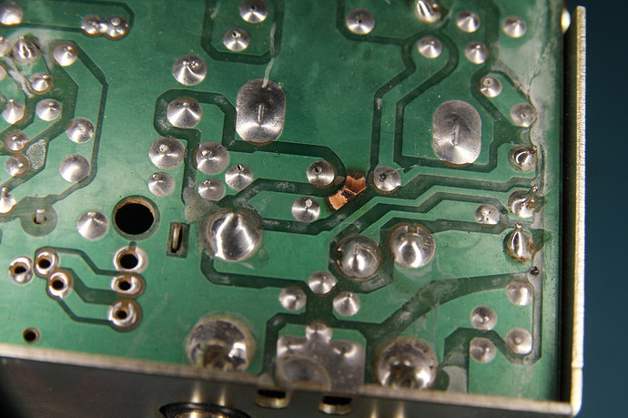 Blown PCB trace caused by reverse polarity in a CB radio, showing the damaged copper.
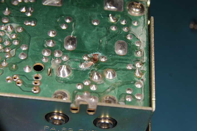
In addition to the trace, the reverse polarity diode can sometimes short out and require replacement. Fortunately, in this instance, the diode was still functioning correctly. With the faulty component identified as the open trace, the printed circuit board repair process could begin.
Step-by-Step PCB Trace Repair Guide
Repairing a blown PCB trace is a straightforward task requiring basic tools and soldering skills. Here’s how to do it:
Step 1: Preparing the Damaged Trace
The first step in printed circuit board repair is to prepare the damaged area. Using a small, precision blade screwdriver, carefully remove the protective coating from the copper trace on both sides of the break. Gently scrape away the coating to expose the bare copper underneath. This ensures a good surface for soldering.
 Preparing a printed circuit board trace for repair by removing the protective coating to expose copper.
Clean both ends of the now exposed copper trace. This removes any debris and further prepares the surface for soldering.
 Close-up of a PCB trace with coating removed, ready for tinning before bridging the gap.
Step 2: Tinning the Copper Trace
Apply a small amount of flux to the exposed copper. Flux is essential in soldering as it cleans the metal surfaces and allows the solder to flow smoothly, creating a strong and reliable joint.
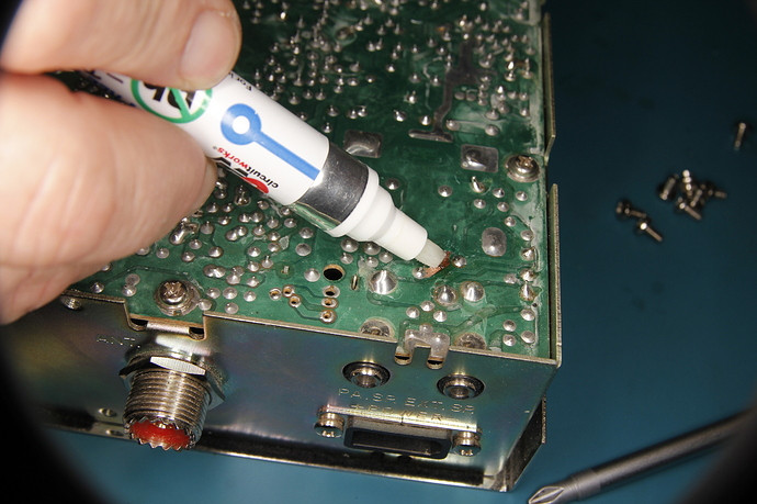 Applying flux to a PCB trace to improve solder flow and adhesion during a circuit board repair.
“Tinning” refers to applying a thin layer of solder to the copper pads. This pre-soldering step makes the final connection easier and improves solder adhesion. Apply a small amount of solder to each exposed copper section until it’s lightly coated.
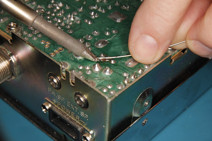
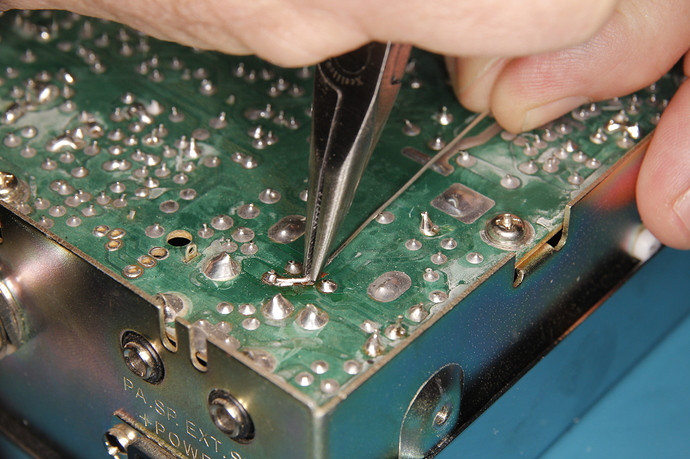
Step 3: Bridging the Gap with Wire
For bridging the broken trace, solid wire, often referred to as bus bar wire, works perfectly. Cut a small piece of solid wire slightly longer than the gap in the trace. Solder one end of the wire to the tinned copper trace on one side of the break.
 Soldering a bus bar wire to one side of a broken PCB trace to create a conductive bridge.
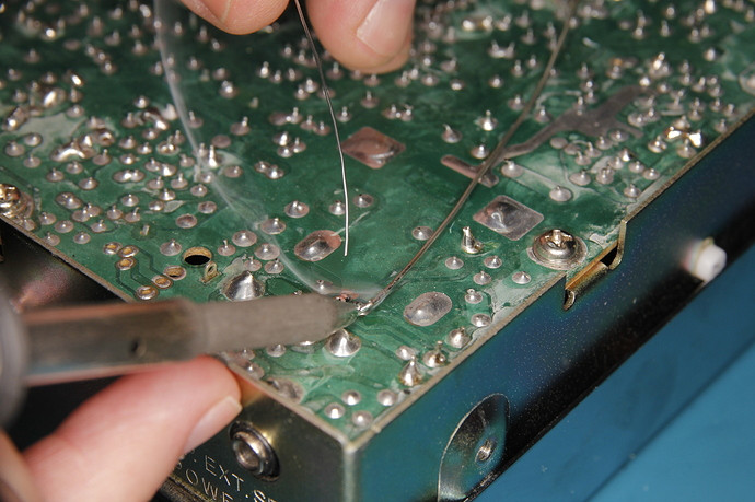
Use needle-nose pliers to carefully bend the wire so it aligns with the other half of the broken trace. Precision here ensures a neat and effective repair.
 Shaping a bus bar wire with pliers to precisely fit the gap in a damaged printed circuit board trace.
Solder the other end of the wire to the remaining tinned section of the trace, completing the electrical bridge across the break.
 Completing a PCB trace repair by soldering the bus bar wire to the second section of the broken trace.
Step 4: Cleaning and Final Check
Trim any excess wire extending beyond the solder joints for a clean finish. Clean the repaired area with flux remover to eliminate any residual flux. Flux residue can sometimes be corrosive or attract dust over time, so removal is important for long-term reliability.
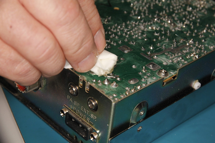 Cleaning soldering flux residue from a repaired PCB trace using flux remover for a clean finish.
The printed circuit board repair is now complete!
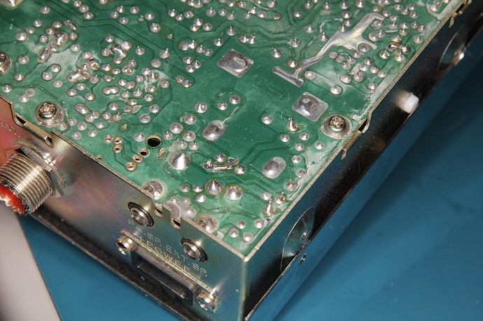 Finished printed circuit board trace repair using a wire bridge, restoring electrical conductivity.
Finally, test the device to ensure the repair was successful. In this case, the CB radio powered up immediately after the printed circuit board repair.
Conclusion
This simple technique of bridging a broken trace is a fundamental skill in printed circuit board repair. Whether dealing with a burnt trace from overcurrent, a fracture on a cracked board, or a trace damaged during component replacement, this method provides an effective solution to restore circuit continuity. By understanding these basic PCB repair techniques, you can extend the life of your electronics and tackle common circuit board issues with confidence.