Printed circuit boards (PCBs) are fundamental to modern electronics, acting as the essential foundation for nearly every electronic device we use. These boards provide the pathways for electrical signals to travel between electronic components, enabling them to function as intended. The demand for high-quality PCBs is constantly increasing as technology advances and consumers expect more sophisticated electronics. This growth is reflected in the global PCB market, which is projected to reach $107.6 billion by 2030 as Manufacturing Printed Circuit boards becomes a more widespread and crucial industry.
Understanding the Printed Circuit Board Manufacturing Process
A printed circuit board, or PCB, is constructed from a non-conductive substrate material upon which conductive pathways, known as traces, are printed or etched. These traces facilitate the connection of electronic components that are mounted onto the board, creating a functional electronic circuit. PCBs are integral to most electronic devices, offering both electrical connectivity and mechanical support for components.
The manufacturing printed circuit board process is a complex industrial undertaking, involving numerous stages of production, inspection, and quality control. This meticulous approach ensures that the final product meets stringent performance requirements. PCBs can be manufactured as single-sided, double-sided, or multilayer boards. While the initial stages of manufacturing are similar for all types, the construction process diverges after the creation of the first conductive layer. Depending on the complexity and design, some PCBs can require over 20 distinct manufacturing steps to be fully realized.
Exploring Different Types of Printed Circuit Board Designs
Printed circuit boards are diverse, categorized by their design specifications, manufacturing methods, and intended applications. Understanding these different PCB types is essential in selecting the appropriate board for a specific electronic device. Here are some of the most common types of PCBs:
Single-Sided PCBs: A Basic Introduction to Circuit Board Manufacturing
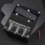
Single-sided PCBs are the most fundamental type of printed circuit board. Characterized by a single conductive copper layer on one side of the substrate, they are a cornerstone of manufacturing printed circuit boards. Electronic components are mounted on one side, leaving the entire etched circuit pattern visible on the opposite side. The limitation of having only one conductive layer means that circuit paths cannot overlap, which can lead to larger board sizes.
 Single-Sided PCB Construction
Description: Illustration showing a cross-section of a single-sided printed circuit board, highlighting the substrate and single copper layer, used in basic electronics manufacturing.
These PCBs are ideally suited for applications with low-density circuit requirements and are frequently used in simple, cost-sensitive electronic devices. Single-sided PCBs are advantageous due to their cost-effectiveness and relative simplicity in design, manufacturing, and repair, making them a popular choice in basic electronics manufacturing.
Double-Sided PCBs: Enhancing Circuit Density in PCB Manufacturing
Double-sided PCBs represent an advancement in manufacturing printed circuit boards, featuring conductive layers on both the top and bottom surfaces of the board. This design allows for increased circuit density and complexity. Connections between the layers are achieved through holes drilled through the board, allowing traces and component pins to link circuits on both sides. Manufacturers utilize various plating methods to establish these interconnections.
The advantages of double-sided PCBs are significant. They enable more compact circuit designs, offer a balance of cost-effectiveness and enhanced functionality, and support higher circuit densities compared to single-sided boards. This makes them well-suited for more sophisticated electronic systems and a common choice in intermediate electronics manufacturing.
Multilayered PCBs: Complexity and High Performance in Circuit Board Manufacturing
Multilayered PCBs represent the pinnacle of complexity in manufacturing printed circuit boards. These boards consist of more than two copper layers, creating a sandwich-like structure where multiple conductive layers are separated by layers of insulating material. The layers are bonded together using lamination under high pressure and temperature, which is crucial for eliminating air gaps and ensuring the structural integrity of the PCB assembly.
Multilayered PCBs are essential for high-speed and high-performance electronic circuits. Their compact nature, compared to single or double-sided options, along with their superior design flexibility and ability to handle complex circuitry, makes them indispensable in advanced electronics manufacturing, including high-speed computing and telecommunications.
Rigid PCBs: Durable and Stable Circuit Boards in Manufacturing
Rigid PCBs are characterized by their solid substrate material, which provides the board with inherent stiffness and strength, preventing bending or flexing. This rigidity is a key feature in manufacturing printed circuit boards where durability and structural stability are paramount. These PCBs are often constructed with multiple layers, including:
- Substrate: The foundation of the PCB, providing structural support.
- Copper Layers: Conductive layers for circuit pathways.
- Solder Mask: A protective layer preventing oxidation and solder bridging.
- Silkscreen: Printed layer for component labels and markings.
These layers are bonded together using adhesives and heat. Rigid PCBs are valued for their ease of diagnostics and repair, vibration resistance, and robust nature. They are widely used in applications ranging from medical equipment to computers, where reliability and stable performance are critical aspects of manufacturing printed circuit boards.
Flex PCBs: Flexible Circuit Solutions in Modern Manufacturing
Flex PCBs are manufactured using flexible substrate materials like polyamide, PEEK, or transparent conductive polyester film, allowing the circuit board to bend and conform to various shapes. This flexibility is a defining characteristic in manufacturing printed circuit boards for applications requiring non-planar or dynamic circuitry. Flex PCBs are available in single-sided, double-sided, and multilayer configurations, offering versatility for diverse applications.
Beyond flexibility, these boards are known for their compact size, high reliability, and manufacturing repeatability. They are particularly advantageous in applications requiring high signal trace density and in devices where space is constrained, making them essential in modern, compact electronic device manufacturing.
A Brief History of Printed Circuit Board Fabrication
The concept of manufacturing printed circuit boards dates back to the early 20th century. German inventor Albert Hansen secured the first patent for a rudimentary PCB in 1903, marking the initial steps in PCB fabrication. Subsequent patents and advancements gradually refined the technology. However, it was in the latter half of the 20th century that significant progress was made, driven by the increasing demand for miniaturization and enhanced functionality in electronics.
The military played a pivotal role in advancing printed circuit board manufacturing techniques. The U.S. Army Signal Corps developed methods to accelerate PCB production through automation, making mass production of PCBs more efficient and cost-effective for consumer electronics. This military influence was crucial in transitioning PCB manufacturing from a niche technology to a mass-production industry.
The past five decades have witnessed remarkable advancements in PCB technology, leading to smaller, lighter, and more functional PCBs. These advancements have enabled the proliferation of portable and multi-functional electronic devices. Today, as we enter an era of unprecedented technological innovation, manufacturing printed circuit boards remains at the forefront, enabling developments from autonomous vehicles to smart homes and beyond.
Key Components of a Printed Circuit Board
A PCB comprises four primary components, each playing a vital role in its function and manufacturing:
- Substrate: Typically made of fiberglass, the substrate provides the structural base of the PCB. It is often considered the most crucial component, offering strength and preventing breakage under stress. In essence, the substrate is the backbone of the PCB, maintaining its integrity.
- Copper Layer: This layer, made of copper foil or coating, is responsible for conducting electrical signals across the PCB. Analogous to the human nervous system, the copper layer facilitates the flow of signals between components. The configuration of the copper layer varies depending on the PCB type.
- Solder Mask: A polymer layer applied over the copper layer, the solder mask acts as a protective skin for the PCB. It prevents copper oxidation, accidental trace damage, and solder bridging during component assembly. While protective, it’s important to note that the solder mask is not designed to function as a dielectric. Solder mask colors can vary and sometimes indicate specific functionalities or production batches.
- Silkscreen: Also known as the legend or nomenclature, the silkscreen is typically printed on the component side of the PCB. It provides essential information such as component part numbers, symbols, switch settings, test points, and component reference designators. This layer aids in assembly, testing, and servicing of the PCB.
The Step-by-Step Manufacturing Process of Printed Circuit Boards
The manufacturing printed circuit board process is a detailed sequence that begins with design and validation and culminates in the fabrication of the physical circuit boards. Precision is paramount at each stage, often requiring computer-controlled and automated machinery to ensure accuracy and prevent defects like short or open circuits. Rigorous testing protocols are essential to verify the functionality of completed PCBs before they are packaged and delivered to customers.
Step One: PCB Design – The Blueprint of Manufacturing
 PCB Design Software Interface
Description: Screenshot of Extended Gerber PCB design software interface, illustrating the digital blueprint creation process for printed circuit board manufacturing.
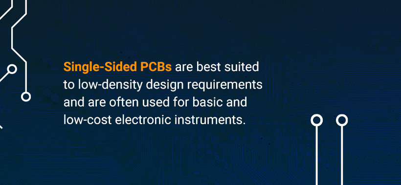
The initial phase in manufacturing printed circuit boards is the design stage. This crucial step involves creating a comprehensive plan that guides the entire manufacturing process. PCB designers use specialized software to develop a detailed blueprint that meets all specified requirements. A widely used software in PCB design is Extended Gerber (IX274X), known for its robust output format.
Extended Gerber software generates all necessary manufacturing data, including the number of copper layers, solder mask requirements, and component notation details. Once the PCB design is encoded in Extended Gerber format, it undergoes thorough checks to identify and rectify any potential errors.
After the designer’s verification, the finalized PCB design is transmitted to a PCB fabrication facility. Here, fabricators conduct a Design for Manufacturing (DFM) check. An effective DFM check is crucial to ensure the design is producible within the facility’s capabilities and will not lead to excessive resource consumption or delays.
Forward-thinking engineers might involve the PCB manufacturer in the DFM process during the design phase. This proactive approach allows for early identification and resolution of manufacturing issues, saving both time and costs. Omissions or critical attribute flaws in the design can negatively impact manufacturing yields.
Step Two: Design Review and Engineering Validation in PCB Manufacturing
A critical stage in the manufacturing printed circuit board process is the design review. This step involves a thorough examination of the PCB design to detect any potential errors, weaknesses, or manufacturability concerns. An experienced engineer meticulously reviews every aspect of the design to ensure no components are missing or incorrectly placed.
Upon passing the engineering review and client approval, the design progresses to the printing phase. Client approval often includes verifying working files, array construction, tooling holes, multi-up array orientation, scoring, and snap-tab details to confirm all specifications are accurately translated into the manufacturing process.
Step Three: Precision Printing for PCB Fabrication
PCB manufacturing employs a unique printing process distinct from conventional document printing. It necessitates specialized plotter printers to produce PCB films. These films serve as photo negatives of the PCB design, crucial for transferring the circuit pattern onto the board.
For inner layers, the plotter printer uses two ink colors:
- Black ink: Represents the conductive circuits and copper traces.
- Clear ink: Indicates non-conductive areas, such as the fiberglass substrate.
This color scheme reverses for outer layers, where clear ink defines copper pathways, and black ink denotes areas where copper will be removed.
Each PCB layer and its corresponding solder mask requires a separate film. Thus, a simple two-layer PCB necessitates four films. After printing, these films are precisely aligned, and registration holes are punched through them using a punch machine. These holes act as alignment guides throughout the subsequent manufacturing steps, ensuring layer registration accuracy.
Step Four: Copper Printing for Interior PCB Layers
In this step of manufacturing printed circuit boards, the physical construction begins. A laminate panel is coated with a photo-sensitive film called resist, composed of photo-reactive chemicals that harden when exposed to ultraviolet (UV) light. The resist enables precise pattern transfer from the PCB blueprint to the laminate.
Using the registration holes for alignment, the resist-coated laminate is exposed to UV light. The UV light passes through the transparent areas of the film, hardening the photoresist underneath, which marks the areas intended to remain as copper traces. Conversely, black ink on the film blocks UV light, leaving the resist unhardened in areas where copper is to be removed.
 Copper Foil Layer Application in PCB Manufacturing
Description: Image of a copper foil layer being applied to a laminate panel in a printed circuit board manufacturing facility, illustrating the initial stage of conductive layer formation.
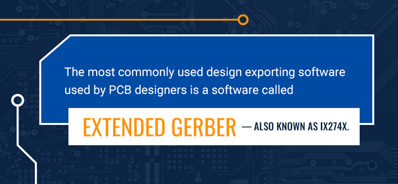
Subsequent to printing the PCB design onto a laminate material, a copper foil layer or copper coating is applied. The copper is pre-bonded to the laminate, forming the PCB’s base. Then, excess copper is etched away to reveal the designed circuit traces.
Inner layers are part of a core structure, consisting of two copper layers with a dielectric material in between. These inner layers are treated with an etch resist before etching to protect the intended copper traces. Post-etching, only the designed copper traces remain.
Following the etching process, the board is washed with an alkaline solution to remove any remaining photoresist and then pressure washed to eliminate any surface particles, before drying. After drying, the remaining resist protects the copper traces. Technicians then inspect the PCB for any defects before proceeding to the next manufacturing step.
Step Five: Etching Inner PCB Layers to Remove Excess Copper
Etching is a crucial step in manufacturing printed circuit boards, particularly for inner layers or cores. It involves selectively removing copper to create the desired circuit patterns. This process entails covering the copper intended to remain as traces and exposing the rest of the board to a chemical etchant. The chemical etching process effectively removes unprotected copper, leaving only the intended circuitry.
The duration and concentration of the copper etching solution may vary based on PCB size and copper weight. Larger PCBs or those with heavier copper layers require more etching, necessitating longer processing times or stronger etchant solutions to ensure complete removal of unwanted copper.
Step Six: Precise Layer Alignment in PCB Manufacturing
After cleaning each PCB layer post-etching, the next critical step in manufacturing printed circuit boards is layer alignment, followed by optical inspection. Registration holes, created earlier, are utilized to precisely align the inner and outer layers. Technicians employ an optical punch machine, which uses pins to accurately align the layers through these registration holes.
Step Seven: Automated Optical Inspection for Quality Assurance in PCB Manufacturing
Following layer alignment, an Automated Optical Inspection (AOI) machine conducts a thorough examination to identify any defects. This AOI step is vital in manufacturing printed circuit boards as it ensures quality control before layers are permanently bonded, at which point errors become irremediable. The AOI system compares the PCB against the Extended Gerber design, acting as the manufacturing standard.
The AOI process verifies that no defects are present. Should any defects be detected by either the technician or the AOI machine, the board is flagged for review or rejection. PCBs that pass AOI proceed to the subsequent stages of manufacturing.
AOI is essential for ensuring the operational reliability of printed circuit boards. It acts as a mid-production quality checkpoint, preventing defective boards with potential short circuits, design specification deviations, or residual copper from advancing further in the manufacturing process. This inspection process is repeated for outer layers after imaging and etching are completed.
Step Eight: Laminating PCB Layers for Structural Integrity
In this stage of manufacturing printed circuit boards, the prepared inner and outer layers are bonded together to form a multilayer PCB structure. Dielectric material is placed between the inner core and the outer layers.
These layers are carefully stacked and clamped using metal clamps on a specialized press table. Each layer is positioned on the table using alignment pins. The lamination process begins with placing a layer of pre-coated epoxy resin, known as prepreg, onto the table. Layers are then built up in a specific sequence: copper foil, dielectric (prepreg), core, dielectric, and copper foil, creating a four-layer “book” configuration.
Once the stack is assembled and a copper press plate is in place, it is moved to a mechanical press, which applies initial pressure to secure the layers. Pins are inserted through the layer stack to maintain alignment. The stack is then transferred to a laminating press. This press uses heated plates to apply both heat and pressure, melting the epoxy in the prepreg and fusing the PCB layer stack together into a cohesive, laminated PCB.
After lamination, the PCB stack is carefully unpacked. The top press plate and alignment pins are removed, allowing the fabricated PCB panel to be extracted.
Step Nine: Precision Drilling of PCBs
Prior to drilling, an X-ray machine is employed to precisely locate drilling positions on the PCB panel. Registration or pilot holes are drilled first to secure the PCB stack for subsequent, more precise drilling operations. Computer-guided drills, using data from the Extended Gerber design, are then used to create all necessary holes, including via holes and component mounting holes.
Following drilling, any excess copper burrs or rough edges along the board edges are removed through a filing or deburring process, ensuring a clean and smooth PCB profile.
Step Ten: PCB Plating for Electrical Connections
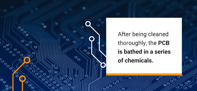 PCB Chemical Bath Plating Process
Description: Image showing a printed circuit board panel being immersed in a chemical bath during the plating process in PCB manufacturing, essential for creating conductive pathways.
After drilling, the PCB panel is prepared for plating. This process is crucial in manufacturing printed circuit boards as it chemically bonds the different layers, establishing electrical connections. The PCB panel undergoes a thorough cleaning process before being immersed in a series of chemical baths. This chemical treatment deposits a thin, micron-thick copper layer across the entire panel surface and into the drilled holes.
Before plating, drilled holes expose the non-conductive fiberglass substrate within the panel. Copper plating covers the walls of these holes, creating conductive pathways between layers. The plating process distinguishes between conductive and non-conductive areas: non-conductive areas are covered with dark ink, while copper areas are coated with light-sensitive ink, facilitating selective plating.
Step Eleven: Outer Layer Imaging for Circuit Definition
In step eleven of manufacturing printed circuit boards, a photoresist layer is applied to the outer layers of the PCB panel, similar to step four for inner layers. This photoresist is specifically applied to the outer layers as they require imaging to define the circuit patterns. Once coated, the outer layers are imaged and then plated, mirroring the inner layer plating process. However, for outer layers, a tin plating is applied over the copper to provide protection during subsequent etching processes.
Step Twelve: Outer Layer Etching to Finalize Circuitry
In the final etching stage for manufacturing printed circuit boards, the tin plating applied in the previous step acts as a protective layer for the underlying copper traces. A copper solvent, similar to that used for inner layers, is used to remove any unwanted copper from the outer layers. The tin plating shields the intended copper circuitry from being etched away. After etching is complete, the protective tin layer is removed.
A key difference between inner and outer layer etching is the area of copper removal. Outer layer etching is a subtractive process where unwanted copper and any remaining resist coating are removed, preparing the outer layers for AOI and solder mask application.
Step Thirteen: Outer Layer Automated Optical Inspection
Similar to inner layers, outer layers of PCBs undergo Automated Optical Inspection (AOI). This inspection is critical in manufacturing printed circuit boards to ensure that the etched outer layers meet design specifications and that all excess copper has been removed. AOI verifies the integrity of the circuit patterns and ensures proper electrical connections will be formed.
Step Fourteen: Solder Mask Application for PCB Protection
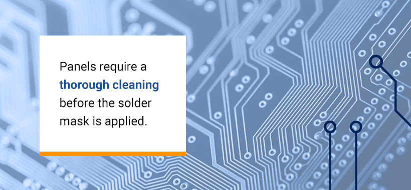 PCB Panels Ready for Solder Mask Application
Description: Image of printed circuit board panels undergoing thorough cleaning prior to solder mask application, a critical step in protecting the copper circuitry.
Before solder mask application, PCB panels must be thoroughly cleaned. The solder mask is then applied using screening or curtain coating techniques and is partially cured (tack-cured). A visual inspection follows, a critical quality control step as many OEMs do not permit solder mask repairs. Defects like voids or inconsistencies necessitate stripping and reapplying the solder mask.
If the solder mask passes inspection, it is fully baked and cured. This cured mask provides crucial protection to the PCB’s copper circuitry against corrosion damage and oxidation. Subsequently, UV light is projected onto the boards to define areas where the solder mask should be removed, a process known as “liquid photo-imageable” solder mask application.
Step Fifteen: Silkscreen Printing and Surface Finish Application
Manufacturing printed circuit boards involves adding critical information directly onto the board surface through silkscreen application, also known as legend printing or nomenclature. This information includes:
- Company identification numbers
- Warning symbols
- Manufacturer logos or marks
- Part numbers
- Pin locators and orientation marks
- Component designators, polarity indicators, and connector pin-outs
This information is typically printed using inkjet printers. Following silkscreen printing, the PCB surface finish is applied. Then, PCBs proceed to testing, cutting, and final inspection phases. For fine details, such as 8-point font or smaller silkscreen text, laser printing is required to ensure legibility.
Step Sixteen: PCB Surface Finishing for Component Assembly
The finishing stage in manufacturing printed circuit boards involves plating the PCB surface with conductive materials to enhance solderability and protect the copper. Common surface finish options include:
- Immersion Silver (ImAg): Offers low signal loss but is prone to oxidation and tarnishing. Lead-free and RoHS compliant.
- Hard Gold (Au): Durable and RoHS compliant, but expensive. Often used for gold fingers on edge connectors.
- Electroless Nickel Immersion Gold (ENIG): A popular finish known for longevity and durability. RoHS compliant and provides excellent flatness for component pads.
- Hot Air Solder Leveling (HASL): Cost-effective and reworkable, but contains lead and is not RoHS compliant.
- Lead-Free HASL: RoHS compliant alternative to HASL, maintaining cost-effectiveness and reworkability. Both HASL types are best suited for devices with 20mm pitch or larger.
- Immersion Tin (ImSn): Suitable for press-fit applications, RoHS compliant, and offers tight hole tolerances. Can present soldering challenges like tin whiskers and has a limited shelf life. Requires controlled storage.
- Organic Solderability Preservative (OSP): RoHS compliant and cost-effective but with a short shelf life.
- Electroless Nickel Electroless Palladium Immersion Gold (ENEPIG): Offers high solder joint strength and prevents nickel corrosion with palladium coating. More expensive and requires precise processing.
The choice of surface finish depends on design requirements and budget. These finishes are essential for enabling component mounting and protecting exposed copper from oxidation.
Step Seventeen: Electrical Reliability Testing for PCB Functionality
After surface finishing and curing, PCBs undergo rigorous electrical testing. These tests must conform to IPC-9252 standards, which outlines guidelines for electrical testing of unpopulated printed boards. The primary tests are circuit continuity and isolation tests. Continuity testing verifies there are no breaks (“opens”) in the circuit paths, while isolation testing checks for shorts between different circuit segments.
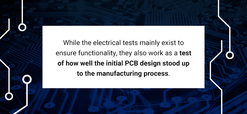 Electrical Testing of Printed Circuit Boards
Description: Image depicting electrical testing of printed circuit boards, highlighting the importance of functional verification in the manufacturing process.
Electrical tests confirm PCB functionality and also validate the manufacturing process against the initial design.
Beyond basic electrical tests, functional tests like the “bed of nails” test may be performed. This test uses spring-loaded probes to apply pressure (up to 200g) to test points on the PCB, assessing the board’s robustness under mechanical stress at contact points.
PCBs that pass electrical reliability testing and any other required tests proceed to the routing and final inspection stages.
Step Eighteen: Profiling and Route Out for PCB Singulation
Profiling, or route out, is the process of separating individual PCBs from the larger manufacturing panel. Fabrication engineers use the shape and size information from the design’s Gerber files to program routing machines. Routing machines create scores or outlines on the construction board, facilitating board separation.
Routing out, or scoring, involves using a router or CNC machine to create small perforations or cuts along the board edges. These scores enable boards to be easily snapped apart without damage. Alternatively, some manufacturers use a v-groove machine to create v-shaped cuts along board edges for separation.
In high-volume manufacturing, a hard-tooled punch may be used to separate PCBs from the panel. Snap-tabs, designed into the customer’s array, can also allow assemblers to detach individual boards after PCB assembly.
Step Nineteen: Final Quality Check and Visual Inspection
After separation, each PCB undergoes a final quality check and visual inspection. This comprehensive inspection verifies:
- Hole Positioning and Tolerances: Hole sizes and locations must match across all layers and meet design specifications.
- Board Dimensions: Overall PCB dimensions must align with the original design.
- Cleanliness: Boards must be free of dust, debris, and contaminants.
- Finish Quality: Edges should be smooth, without burrs or sharp points.
- Electrical Reliability: Any boards that failed earlier electrical tests are re-evaluated after repairs.
Step Twenty: Packaging and Secure Delivery of PCBs
The final step in manufacturing printed circuit boards is packaging and delivery. PCBs are typically vacuum-sealed in moisture-barrier bags to protect against dust and contaminants. These sealed packages are then placed in protective containers to prevent physical damage during shipping. Depending on customer specifications, electrostatic discharge (ESD) protective packaging may be used to prevent static damage during transit. Finally, the packaged PCBs are shipped to the customer.
Manufacturing Multilayer Printed Circuit Boards: Additional Considerations
Manufacturing multilayer printed circuit boards involves additional steps to accommodate the multiple copper layers and cores. Key additions include bonding and lamination under high temperatures and pressures to eliminate air gaps between layers. These processes are crucial for ensuring the stability and reliability of the multilayer PCB assembly.
Inner Layer Imaging in Multilayer PCB Manufacturing
Inner layer imaging for multilayer PCBs follows the same procedures as described for standard PCB design printing. The design is printed on a plotter printer to create a film, including the solder mask for the inner layer. Registration holes are created in the films to ensure precise alignment during subsequent steps.
Copper is added to the laminate material for the inner layer, and the printed film is placed over the laminate, aligned using the registration holes. UV light exposure hardens the photoresist in the transparent areas of the film, creating the printed circuit pattern. These hardened areas will resist removal during etching, while unhardened areas under dark film will have their copper removed.
Inner Layer Etching in Multilayer PCB Manufacturing
Following imaging, the areas exposed to clear ink are hardened, protecting the copper underneath during etching. Technicians wash the board with an alkaline solution to remove unhardened resist. Then, the board is immersed in a copper solvent to etch away excess copper from non-conductive areas, leaving the intended circuit patterns defined by the hardened resist.
Resist Stripping in Multilayer PCB Manufacturing
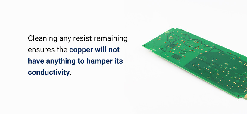 Resist Stripping Process in PCB Manufacturing
Description: Image depicting the resist stripping process in printed circuit board manufacturing, where remaining photoresist is removed to ensure clean copper conductivity.
Resist stripping is the step where any remaining resist covering the copper of the PCB inner layer is removed. Removing all resist ensures unimpeded copper conductivity. After resist stripping, the inner layer is ready for quality inspection.
Post Etch Punch in Multilayer PCB Manufacturing
The post-etch punch step aligns layers and punches registration holes using computer-guided optical punch machines. These holes are crucial for accurate layer alignment in subsequent lamination and drilling processes.
Inner Layer AOI in Multilayer PCB Manufacturing
Inner layer Automated Optical Inspection (AOI) is performed using computer-controlled systems to meticulously examine each inner layer. AOI checks for incomplete circuit patterns or residual resist. Layers passing AOI proceed to the next stage of multilayer PCB manufacturing.
Inner Layer Oxide Treatment in Multilayer PCB Manufacturing
Oxide treatment is applied to the inner copper layers to enhance bonding between copper foil and insulating epoxy resin layers in multilayer PCBs. This treatment improves layer adhesion and overall PCB reliability.
Layup Process in Multilayer PCB Manufacturing
The layup step in multilayer PCB manufacturing involves automated machinery to precisely align, heat, and bond PCB layers. Copper foil and insulating prepreg layers are placed between inner and outer layers. Alignment pins, based on post-etch registration holes, secure the layers before lamination. Computer-controlled machines ensure accurate layer alignment and bonding.
Lamination of Multilayer PCBs
Lamination is a critical process step that uses heat and pressure to melt the epoxy bonding material (prepreg) between layers. Properly laminated PCBs maintain tight layer bonding, providing robust insulation and structural integrity to the final product.
X-Ray Alignment for Multilayer PCB Drilling
When drilling multilayer PCBs after lamination, X-ray alignment is used to precisely position the drill bit. Accurate hole placement is crucial for interlayer connections. Following X-ray alignment, the multilayer PCB undergoes drilling and then follows the subsequent manufacturing steps common to single and double-sided PCBs.
Implementing Effective PCB Manufacturing Processes
The design and manufacturing processes of PCB fabrication often involve collaboration between different entities. Contract manufacturers (CMs) typically assemble PCBs designed by original equipment manufacturers (OEMs). Effective collaboration between OEMs and CMs on component selection, design considerations, file formats, and board materials is essential for a streamlined and efficient manufacturing process.
Design for Manufacturing (DFM) Considerations in PCB Manufacturing
Design for Manufacturing (DFM) is a critical approach that considers how well a PCB design can be produced through the various stages of fabrication. PCB fabricators often have DFM guidelines that OEMs can consult during the design phase. Designers should request these guidelines to ensure their PCB designs are optimized for the specific fabricator’s production capabilities.
Designers should also consult with fabricators about available materials. Ideally, fabricators should have all necessary components readily available. If material constraints arise, designers and fabricators must collaborate to find compromises that ensure efficient manufacturing while still meeting essential design specifications.
File Format Standardization in PCB Manufacturing
Clear communication and data exchange between OEMs, CMs, and PCB manufacturers are crucial. Using standardized file formats for PCB designs is essential to prevent errors and data loss during file transfers and conversions. Consistent file formats ensure accurate translation of design specifications into manufacturing instructions.
Material Selection and Availability in PCB Manufacturing
OEMs may specify materials that are more expensive or less readily available than standard materials anticipated by PCB manufacturers. Early agreement on materials is vital. OEMs and manufacturers must align on material choices that meet design requirements while also being cost-effective and available within the manufacturing timeline.
Why Choose Amazing Print for Your PCB Manufacturing Needs?
As a content creator for amazingprint.net, we aim to provide valuable insights into the world of manufacturing printed circuit boards. While we focus on content creation, understanding the complexities of PCB manufacturing is crucial in today’s technology-driven world.
Millennium Circuits Limited (MCL), as referenced in the original article, is a reputable PCB supplier with extensive experience since 2005. They emphasize customer service, rapid response, and technical support, catering to diverse industries. Their focus on customer satisfaction and streamlined processes aligns with the values of providing high-quality and efficient services.
Understanding the intricate processes involved in manufacturing printed circuit boards underscores the value and effort invested in each board. For businesses seeking PCB manufacturing services, it is essential to partner with reliable and experienced manufacturers who prioritize quality and customer needs.
Contact Us for More Information on PCB Manufacturing
High-quality PCB engineering and manufacturing are vital for the success of electronic products. A thorough understanding of the manufacturing process highlights the complexities and the critical importance of each step in producing a functional printed circuit board.
For further inquiries about PCB manufacturing or to explore potential collaborations, [contact us at amazingprint.net]([Insert Contact Link Here]). We are committed to providing informative content and connecting you with resources and expertise in the field of printed circuit board manufacturing.