
Electronics are the backbone of modern life, powering everything from the smartphones in our pockets to the complex systems within our vehicles. At the heart of almost every electronic device lies the printed circuit board (PCB). You’ve likely encountered these green or sometimes other colored boards, adorned with intricate lines and metallic components, when peering inside discarded electronics. PCBs are typically constructed from fiberglass, interwoven with copper traces and various metallic elements, bound together by epoxy, and shielded with a solder mask that often lends them their distinctive green hue.
However, a bare PCB is only the starting point. A circuit board’s true potential is unlocked when electronic components are precisely mounted onto it. This transformation turns a simple PCB into a functional Printed Circuit Assembly (PCA), often referred to as PCBA. The process of attaching these components is known as PCB assembly, or PCBA for short. The copper traces on the bare board, acting as electrical pathways, connect components and connectors, enabling signals to flow and the circuit board to perform its designed functions. These functions can range from the simplest circuits to incredibly complex systems, all within a space that can be smaller than your thumbnail.
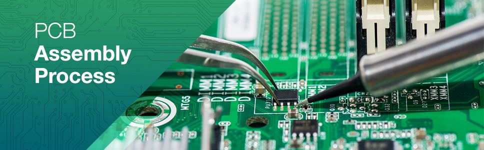
But how are these intricate assemblies actually created? The printed circuit assembly process is a well-defined series of steps, blending automated precision with manual expertise. Throughout each stage, PCB manufacturers can choose between automated and manual methods, depending on factors like volume, complexity, and cost. To provide a clear understanding of how a PCBA comes to life, let’s delve into each step of the process, from start to finish.
 PCB Assembly Process | PCBCart
PCB Design Fundamentals for Assembly
The PCBA journey begins with the fundamental building block: the PCB itself. A PCB isn’t just a single layer; it’s typically a multi-layered structure, each layer contributing to the overall functionality of the final printed circuit assembly. These layers are carefully constructed and include:
- Substrate: This is the foundational layer, the base material that gives the PCB its structural rigidity. It’s the backbone upon which all other layers are built.
- Copper Layers: A thin layer of conductive copper foil is applied to one or both sides of the substrate, depending on whether it’s a single-sided or double-sided PCB. This copper layer is then etched to create the conductive traces, the pathways for electrical signals.
- Solder Mask: Positioned on top of the copper layer, the solder mask is a protective coating that insulates the copper traces, preventing unintended contact with other conductive materials, which could lead to short circuits. It also defines the areas where solder will be applied. The solder mask is responsible for the characteristic green color of many PCBs. Openings in the solder mask, known as solder pads, are where components will be soldered to the board.
- Silkscreen: The outermost layer is the silkscreen, typically white, which is used to print labels, component designators, logos, and other information onto the PCB. This layer is crucial for assembly, testing, and servicing, as it helps identify component locations and functions.
While these materials and components are generally consistent across most PCBs, the substrate material can vary significantly. The choice of substrate depends on the desired characteristics of the final product, such as cost, flexibility, and thermal performance.
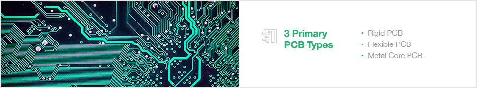
PCBs are broadly categorized into three primary types based on their substrate:
 PCB Types | PCBCart
- Rigid PCBs: These are the most common type, forming the majority of printed circuit assemblies. Their solid core provides stiffness and thickness. The most prevalent material for rigid PCBs is fiberglass, specifically FR-4, known for its balance of cost, durability, and electrical properties. Less expensive options like epoxies or phenolics are also used but offer reduced durability compared to FR-4.
- Flexible PCBs (Flex PCBs): Offering greater pliability, flexible PCBs are made from bendable, high-temperature plastics like Kapton. These are ideal for applications requiring flexibility, such as in wearable electronics or tight spaces.
- Metal Core PCBs (MCPCBs): These PCBs utilize a metal core, typically aluminum, to efficiently dissipate heat. MCPCBs are particularly beneficial for applications generating significant heat, protecting sensitive components and improving overall reliability.
Furthermore, component mounting technologies play a crucial role in printed circuit assembly. Two dominant technologies are used in modern PCBA:
 Thru-hole technology | PCBCart
- Surface Mount Technology (SMT): SMT involves mounting components, known as Surface Mount Devices (SMDs), directly onto the surface of the PCB. SMDs are often small, and SMT is well-suited for high-density assemblies and miniaturization. Automated pick-and-place machines precisely position SMDs onto solder paste, which is then reflowed to create permanent connections. Modern SMT lines can handle incredibly small components, down to 01005 size, smaller than a pencil point.
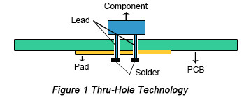
- Through-Hole Technology (THT): THT is used for components with leads or pins that are inserted through pre-drilled holes in the PCB. The leads are then soldered on the opposite side of the board. THT provides stronger mechanical connections and is often used for larger, heavier components like connectors, capacitors, and inductors that require robust attachment.
 Thru-hole components | PCBCart
Because of the differences between SMT and THT, their assembly processes differ significantly. Modern printed circuit assembly often utilizes a combination of both technologies, known as mixed technology assembly, to leverage the strengths of each.
Pre-Assembly Preparations: Design for Manufacturability (DFM) Check
Before the physical PCB assembly process begins, several crucial preparatory steps are essential. These steps ensure the PCB design is functional, manufacturable, and optimized for efficient assembly. A primary step is the Design for Manufacturability (DFM) check.
Most PCB assembly companies require the PCB design files, along with any specific design notes and requirements, to initiate the process. This allows them to conduct a comprehensive DFM check. The DFM check is a critical analysis of the PCB design files to identify any potential issues that could impact the PCB’s functionality or its ease of manufacturing.
 DFM Check | PCBCart
The DFM check scrutinizes all aspects of the PCB design specifications, looking for missing information, redundancies, or potential problem areas. Common design flaws, such as insufficient spacing between components, can lead to short circuits and malfunctions.
By proactively identifying and addressing potential issues before manufacturing commences, DFM checks significantly reduce manufacturing costs and prevent unforeseen expenses. This is achieved by minimizing the number of scrapped boards due to design errors. Leading PCB assembly providers, like PCBCart, often include a free DFM check as a standard part of their service, demonstrating their commitment to quality and cost-effectiveness. Advanced DFM tools, like Valor DFM/DFA, provide automated, high-speed, and accurate analysis, further enhancing the efficiency and reliability of the printed circuit assembly process.
The Actual PCBA Process: Step-by-Step
With the design validated and optimized, the physical PCBA process unfolds in a series of carefully orchestrated steps:
Step 1: Solder Paste Stenciling
The first step in PCB assembly is applying solder paste to the PCB. This is analogous to screen-printing, where a thin, stainless steel stencil is precisely aligned over the PCB. The stencil has openings that correspond to the pads on the PCB where components will be placed. Solder paste is then applied through these openings.
 Solder Paste Composition | PCBCart
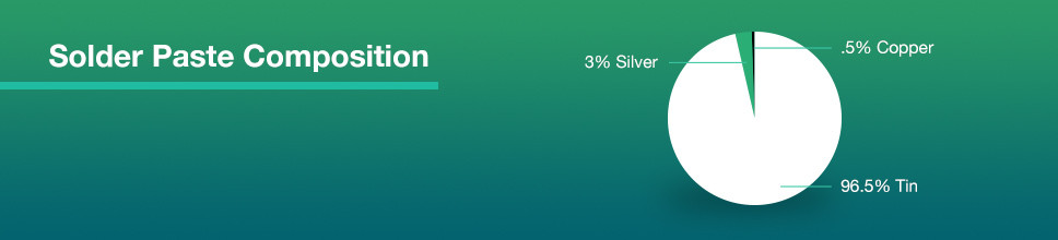
Solder paste is a viscous, greyish material composed of tiny solder balls (typically 96.5% tin, 3% silver, and 0.5% copper) mixed with flux. The flux is a chemical agent that facilitates the soldering process by cleaning the metal surfaces and promoting the flow and wetting of the molten solder. Accurate and consistent solder paste application is crucial for reliable solder joints.
In a professional PCBA line, automated stencil printers are used for this step. The PCB is secured in a fixture, the stencil is precisely positioned, and solder paste is automatically dispensed and spread across the stencil using a squeegee. After stenciling, the stencil is carefully removed, leaving solder paste only on the designated pads, ready for component placement.
Step 2: Component Placement (Pick and Place)
Following solder paste application, the PCB moves to the pick and place machine. This automated robotic system precisely places Surface Mount Devices (SMDs) onto the PCB, aligning them with the solder paste-printed pads. SMDs constitute the majority of components in modern printed circuit assemblies, excluding connectors.
Historically, component placement was a manual and painstaking process, requiring assemblers to use tweezers to hand-place each component. Modern PCB assembly overwhelmingly utilizes automated pick and place machines due to their superior accuracy, speed, and consistency. Machines operate tirelessly, eliminating human fatigue and the associated errors, especially when dealing with increasingly miniaturized components.
 Surface Mount Technology | PCBCart
The pick and place machine uses vacuum nozzles to pick components from feeders (reels or trays) and precisely position them onto the PCB pads, guided by pre-programmed coordinates. The components are gently placed onto the solder paste, which acts as a temporary adhesive, holding them in place for the next step.
Step 3: Reflow Soldering
With solder paste and SMDs in position, the next step is to create permanent solder joints. This is achieved through reflow soldering. The PCB is conveyed through a reflow oven, a long, tunnel-like oven with multiple heating zones.
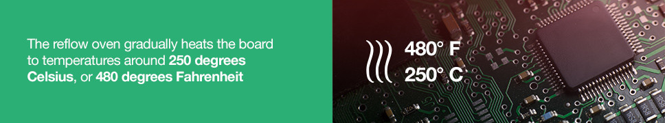 Reflow Soldering | PCBCart
The reflow oven precisely controls the temperature profile the PCB experiences. It typically involves a pre-heating zone, a soak zone, a reflow zone where the temperature peaks (around 250°C or 480°F, sufficient to melt the solder), and a cooling zone. The controlled heating and cooling process ensures the solder paste melts and wets the component leads and PCB pads, forming reliable solder joints as it solidifies.
For two-sided PCB assemblies, each side is typically processed separately. The side with fewer and smaller components is usually processed first, followed by the other side to minimize component displacement during the reflow process.
Step 4: Inspection and Quality Control
After reflow soldering, the printed circuit assembly is not yet complete. Inspection and quality control are crucial to identify and rectify any defects. The reflow process can sometimes lead to issues like poor solder joints, missing components, misaligned components, or solder bridges (shorts).
 Inspection and Quality Control Methods | PCBCart
Several inspection methods are employed:
- Manual Visual Inspection: For small batches or prototypes, manual inspection by trained technicians is often performed. They visually examine solder joints, component placement, and overall assembly quality. However, manual inspection is subjective and prone to errors, especially for complex and high-volume assemblies.
- Automated Optical Inspection (AOI): AOI is widely used for larger production volumes. AOI systems use high-resolution cameras and image processing algorithms to automatically inspect PCBs. They compare images of the assembled PCB to a known good reference, detecting defects like missing components, incorrect components, misalignments, solder joint defects, and more. AOI is fast, objective, and significantly improves quality control.
- X-ray Inspection: For complex, multi-layered PCBs, and especially for Ball Grid Array (BGA) packages where solder joints are hidden beneath the component, X-ray inspection is employed. X-ray inspection allows visualization of solder joints beneath components and within multi-layer boards, detecting hidden defects like voids or insufficient solder.
Defective boards are either reworked (repaired) or scrapped, depending on the nature and severity of the defect and the PCB assembly company’s quality standards.
Step 5: Through-Hole Component Insertion
Depending on the design, the printed circuit assembly may include through-hole components (PTH components) in addition to SMDs. PTH components require different assembly and soldering methods.
Unlike SMDs, PTH components have leads that are inserted into holes drilled through the PCB. Solder paste is not suitable for PTH components as it would simply flow through the holes. PTH component soldering typically employs two main methods:
- Manual Soldering: For low-volume production or when only a few PTH components are present, manual soldering is used. Technicians insert PTH components into the designated holes and then manually solder the leads on the underside of the board using soldering irons. Manual soldering is labor-intensive but provides flexibility for complex or low-volume assemblies.
- Wave Soldering: For higher volume PTH assembly, wave soldering is an automated process. After PTH components are inserted, the PCB is passed over a wave of molten solder. The wave of solder contacts the underside of the PCB, soldering all PTH component leads simultaneously. Wave soldering is efficient for PTH components but is generally not suitable for double-sided assemblies with SMDs on both sides, as the molten solder wave could damage SMDs on the bottom side.
After PTH soldering, another round of inspection may be performed to ensure the quality of through-hole solder joints.
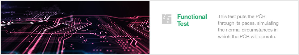
Step 6: Final Inspection and Functional Testing
The final step in the PCBA process is the functional test. This test verifies that the assembled PCB functions as intended. Functional testing simulates the operating conditions of the PCB and checks if it meets the required performance specifications.
 Functional Test | PCBCart
During functional testing, power is applied to the PCBA, and input signals are provided while output signals and other parameters (voltage, current, signal characteristics) are measured and monitored. The test procedure is specific to the design and function of the PCB. Any PCBA that fails the functional test is rejected and may be further analyzed for root cause and potential rework or scrapped.
Functional testing is the ultimate validation of the PCB assembly process and ensures that only working and correctly assembled PCBs are shipped to customers.
Post-Assembly Processes: Cleaning
After soldering and testing, the printed circuit assembly process is nearly complete. However, a crucial post-assembly step is cleaning. Soldering processes leave flux residue on the PCB, and handling during assembly can introduce contaminants like oils and dirt.
Flux residue can be aesthetically unappealing and, more importantly, can be corrosive over time, potentially damaging solder joints and affecting long-term reliability. Cleaning removes flux residue and other contaminants, improving the appearance and long-term performance of the PCBA.
Automated PCB cleaning systems, typically using deionized water and specialized cleaning agents, are employed. Deionized water is used because it lacks ions that could be conductive and potentially damage the circuit. High-pressure spray and immersion cleaning methods are common. After cleaning, a drying cycle, often using compressed air, removes moisture and prepares the PCBs for packaging and shipment.
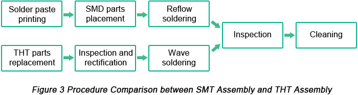
Differences in PCBA Processes: THT, SMT, and Mixed Technology Assembly
The printed circuit assembly process varies depending on the component mounting technologies used: Through-Hole Technology (THT), Surface Mount Technology (SMT), or a combination of both (Mixed Technology).
 Procedure Comparison between SMT Assembly and Thru-hole Assembly | PCBCart
Through-Hole Technology (THT) Assembly Process:
THT assembly is a more traditional method, often involving a blend of manual and automated steps.
- Step 1: Component Placement: Typically manual, where trained technicians insert PTH components into the correct locations on the PCB, following design files and assembly instructions. Attention to component orientation, polarity, and handling of static-sensitive components is crucial.
- Step 2: Inspection & Rectification: After manual placement, PCBs are often inspected to verify correct component placement before soldering. Errors can be easily corrected at this stage.
- Step 3: Wave Soldering: The primary soldering method for THT components. PCBs with placed components are conveyed over a wave of molten solder, which solders all PTH leads simultaneously.
Surface Mount Technology (SMT) Assembly Process:
SMT assembly is characterized by its high degree of automation and efficiency.
- Step 1: Solder Paste Printing: Solder paste is precisely applied to the PCB pads using a stencil printer. Solder paste inspection (SPI) may be performed to ensure print quality.
- Step 2: Component Mounting (Pick and Place): Automated pick and place machines mount SMDs onto the solder paste.
- Step 3: Reflow Soldering: PCBs with placed SMDs are passed through a reflow oven to melt the solder paste and create permanent solder joints.
Mixed Technology Assembly:
Modern electronics often require both SMT and THT components on the same PCB, leading to mixed technology assembly. This requires careful process planning to optimize assembly efficiency and quality.
Mixed technology printed circuit assembly scenarios include:
- Single-Sided Mixed Assembly: SMT and THT components on the same side of the PCB. Typically, SMT components are assembled first using SMT processes, followed by manual insertion and wave soldering of THT components. Hand soldering can be used for small numbers of THT components.
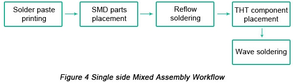 Single-side Mixed PCB Assembly Workflow | PCBCart
- One Side SMT & One Side THT: SMT components on one side of the PCB and THT components on the other. This approach is less common due to increased complexity and potential soldering challenges. Adhesives may be required to hold SMT components during THT wave soldering, adding cost and complexity.
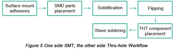 One side SMT, the other side Thru-hole Assembly workflow | PCBCart
- Double-Sided Mixed Assembly: SMT and THT components on both sides of the PCB. This is the most complex type of mixed assembly. Options include using adhesives to mount components on the bottom side before wave soldering, or selective soldering techniques to avoid soldering components already placed on the top side. Double-sided mixed assembly often involves multiple soldering steps and can be less efficient.
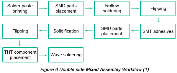 Double side Mixed PCB Assembly workflow (with adhesives) | PCBCart
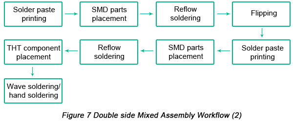 Double side Mixed PCB Assembly workflow (without adhesives) | PCBCart
Choosing the right PCB assembly process and technology mix is crucial for cost-effectiveness, efficiency, and product quality. Factors like component types, volumes, design complexity, and budget all influence the selection of assembly methods.
Partnering with PCBA Professionals
Printed circuit assembly is a complex and technical process requiring expertise, precision, and careful attention to detail. Selecting a reliable and experienced PCB assembly partner is critical for ensuring the success of your electronic product.
PCBCart is a leading provider of comprehensive PCB solutions, offering services from PCB fabrication to full turnkey electronic assembly. They provide expertise and quality assurance throughout every stage of the process.
 Full Turnkey PCB Assembly Service | PCBCart
By choosing PCBCart as your PCBA partner, you gain access to a service committed to the highest quality standards, meeting IPC Class 3, RoHS, and ISO 9001:2008 certifications. They are equipped to handle diverse PCB types, including single-sided, double-sided, SMT, through-hole, and mixed-technology assemblies.
PCBCart emphasizes consistent communication throughout the project, keeping you informed from design to completion. This collaborative approach can lead to cost savings, reduced lead times, and higher-quality printed circuit assemblies, allowing you to focus on your designs and innovations, confident in the manufacturing process.
Explore further resources to deepen your understanding of Electronic Assembly and PCBCart’s capabilities:
- A Comprehensive Introduction of PCBA
- How to Evaluate PCB Assembly Houses?
- PCBCart Offers Advanced Turnkey PCB Assembly Service without MOQ Requirement
- Design for Manufacture and Assembly of PCBs and General Rules It Conforms to
- Design PCBs to Better Take Advantage of PCBCart’s PCB Assembly Capabilities
- Instruction on Getting Precise PCB Assembly Prices