
Printed circuit board (PCB) design has evolved into a highly specialized domain within the electronics industry. PCBs are fundamental components, acting as the backbone of nearly every electronic device we use daily. They serve several critical functions: providing electrical connections between electronic components, offering rigid support for component mounting, and enabling compact packaging for integration into finished products. In essence, the PCB is the central element in any electronic device, dictating its form and functionality, and facilitating high-speed communication between advanced semiconductors.
What Exactly is a Printed Circuit Board?
A printed circuit board, or PCB, is best understood as an electronic assembly that utilizes copper conductors to establish electrical pathways between various components. Beyond electrical connectivity, PCBs also provide essential mechanical support, allowing electronic components to be securely mounted within a device enclosure.
PCBs are constructed from layered materials, alternating between conductive copper layers and electrically insulating layers. The conductive elements on a PCB include copper traces (circuit pathways), pads (connection points for components), and conductive planes (larger areas for power and ground). The structural integrity comes from the insulating material that is laminated between these conductive layers. The entire structure undergoes plating and is then coated with a non-conductive solder mask. Finally, a silkscreen legend is printed atop the solder mask, providing component identification and markings for assembly. After these fabrication processes are complete, the bare PCB is ready for printed circuit board assembly (PCBA), where electronic components are soldered onto the board and the PCBA undergoes testing.
During the PCB manufacturing process, the inner copper layers are meticulously etched. This etching process removes unwanted copper, leaving behind the precise traces required to connect components within the circuit board. Multiple etched layers are then carefully laminated together in a sequential process until the desired PCB stack-up is achieved. This stack-up represents the complete layering structure of the PCB. This entire process defines PCB fabrication, resulting in a bare board ready for the subsequent printed circuit board assembly phase.
A Journey Through PCB History
To truly appreciate modern PCB design, it’s helpful to understand the historical context from which PCBs emerged.
In the early days of electronics, circuits were constructed using individual integrated circuits (ICs) and discrete components. These components were interconnected using wires, and mounted onto a rigid base material, originally often bakelite. Bakelite was initially chosen as a replacement for plywood in certain applications. However, as circuit complexity grew, the sheer number of wires became problematic. Wiring became tangled, bulky, and debugging complex circuits was a nightmare. Reliability suffered, and manual soldering of numerous components and wires made manufacturing slow and labor-intensive.
Early PCBs often resembled the example below, characterized by exposed copper traces and numerous through-hole components, which were larger and bulkier than today’s surface mount components.
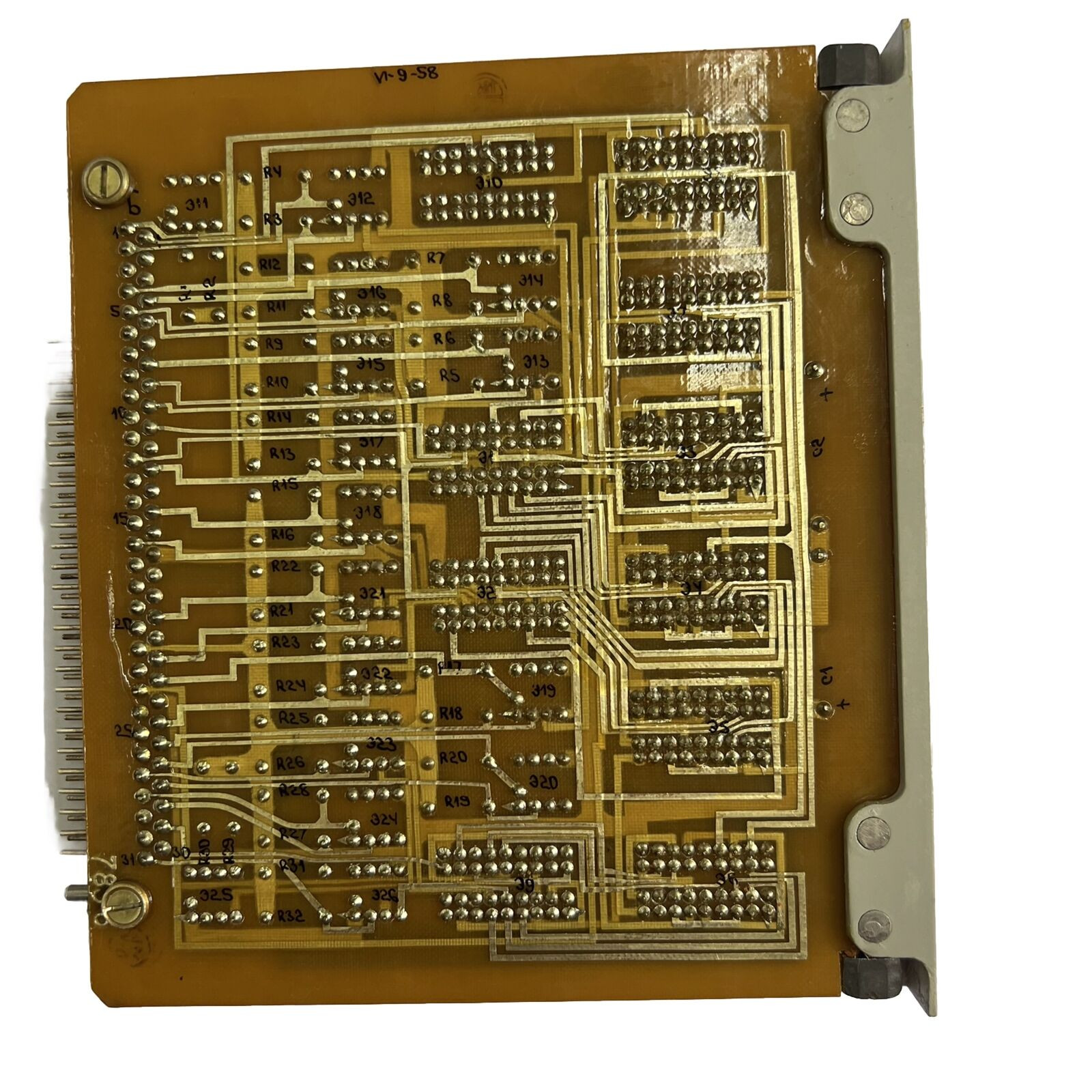 An example of an older PCB with through-hole components
Modern electronics, in stark contrast, often involve incredibly dense designs with a multitude of tiny components. These include miniature ICs, extremely small passive components, and advanced chips boasting very high pin counts. Manually wiring these components is simply impractical. Instead, copper connections are directly deposited onto insulating substrates, as described in the modern manufacturing process. Today’s devices are frequently advanced high-density interconnect (HDI) designs, featuring thousands of connections and numerous electrical interfaces. PCBs power a vast array of devices, from smartphones and heart rate monitors to complex systems like rockets.
Diverse Types of PCBs
While rigid PCBs are the most common, constructed on solid substrates, a variety of other PCB types exist, built on different materials and offering unique characteristics. Common PCB types include:
- Rigid PCBs: These are the most common type, made from solid, inflexible materials like fiberglass-reinforced epoxy resin (FR-4). They are used in a wide range of applications due to their cost-effectiveness and durability.
- Flexible PCBs (Flex PCBs): Constructed on flexible substrates like polyimide film, flex PCBs can bend and fold. They are ideal for applications requiring flexibility, such as in wearable devices, foldable electronics, and automotive applications.
- Rigid-Flex PCBs: These combine rigid and flexible PCB technologies into a single board. Rigid sections provide component mounting and support, while flexible sections allow for bends and folds to connect different parts of a device, reducing the need for connectors and wiring.
- Multilayer PCBs: These PCBs have more than two copper layers, allowing for increased circuit density and complexity. They are used in advanced electronics like computers, smartphones, and high-speed communication systems.
- Single-Layer PCBs: These are PCBs with a single conductive layer. They are simple and cost-effective, suitable for basic electronic devices.
- Double-Layer PCBs: These PCBs have conductive layers on both sides of the substrate, increasing circuit density compared to single-layer PCBs.
Modern Electronic Computer-Aided Design (ECAD) software empowers designers to create any of these PCB types, provided the correct PCB design rules and manufacturing constraints are implemented within the software.
 An older PCB with through-hole components
Older circuit boards predominantly used through-hole components in their design. The image above illustrates an older circuit board relying heavily on through-hole components to achieve its functionality. Modern printed circuit boards have largely transitioned to surface-mount devices (SMD) due to their suitability for high-density, double-sided designs. SMD components are now the standard choice for applications prioritizing small form factor, low power consumption, and cost-effectiveness. However, through-hole components still find use in certain applications where robustness, reliability, and ease of assembly, including manual assembly, are paramount. The image below showcases a contemporary PCB populated with high-density SMD components.
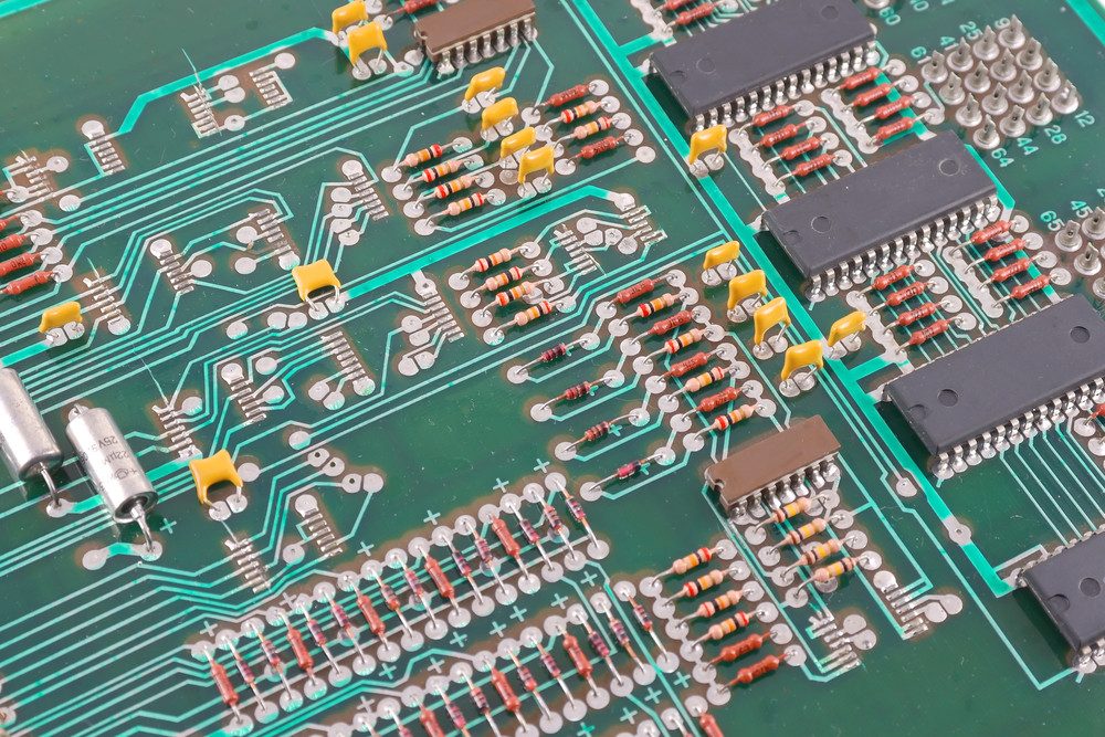
 A modern PCB with surface mount components
Modern printed circuit board designs frequently incorporate surface mount components and various solder mask colors.
PCB Structure and Diverse Applications
Many critical performance characteristics of a PCB are defined by its layer stack-up, which is the arrangement of conductive and insulating layers. The stack-up involves alternating layers of conductive material (copper) and insulating materials, typically core and prepreg. Core and prepreg are types of dielectric materials used in PCB construction. The dielectric and mechanical properties of the core and prepreg materials are crucial as they directly influence the reliability and signal/power integrity of the PCB design. Careful material selection is paramount, especially in high-reliability applications. For instance, PCBs designed for military or medical devices, which may operate in harsh environments, demand highly reliable materials. Similarly, a PCB intended for a telecom system might necessitate a low-loss PTFE laminate to ensure signal integrity within a compact size.
A typical PCB stack-up example is shown below. This example demonstrates a 4-layer structure with two internal plane layers: one for ground (L02_GND) and one for power (L03_PWR). This type of stack-up is well-suited for IoT (Internet of Things) devices, lightweight embedded systems, and numerous other designs employing high-speed communication protocols. The internal plane arrangement enhances power integrity and provides a degree of shielding against external electromagnetic interference (EMI). Furthermore, these internal planes act as consistent references for controlled impedance signals, which are essential for high-speed signal transmission. This 4-layer configuration is a common starting point for many modern printed circuit board designs.
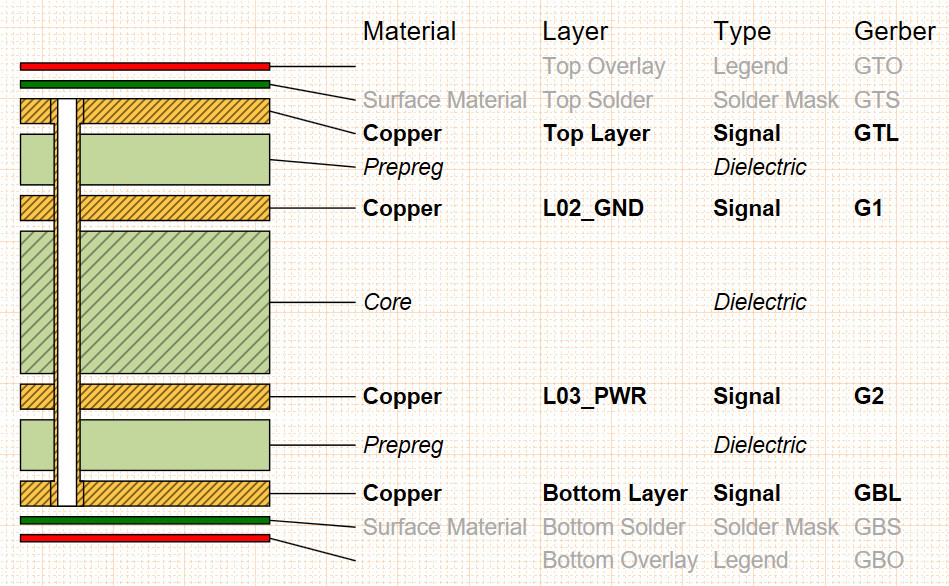 Example of a 4-layer PCB stack-up
Example stack-up drawing created with Draftsman in Altium Designer.
High-Density Interconnect (HDI) PCB Design
Modern advanced electronic devices increasingly utilize high-density interconnect (HDI) PCB design practices. HDI PCBs are characterized by extremely small feature sizes, enabling higher component density and increased functionality in smaller form factors. While the fundamental engineering principles remain similar to standard PCBs, HDI PCBs are typically employed in more sophisticated systems requiring a large number of components and interconnections. Prominent examples of products incorporating HDI PCBs include:
- Smartphones and mobile devices
- Data center infrastructure, such as server motherboards
- Add-in cards for servers and embedded computers
- Miniaturized medical wearables and implantable devices
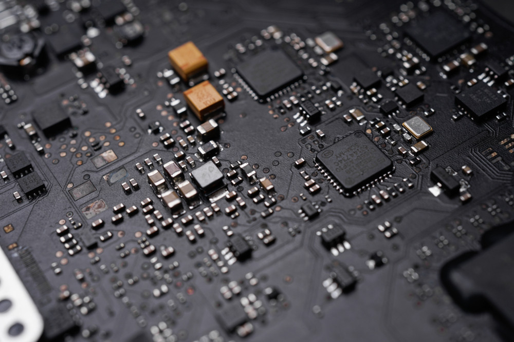
A key component packaging technology driving the adoption of HDI PCB design and manufacturing is ball grid array (BGA) packaging, along with related packages like land grid array (LGA). Many microcontrollers, microprocessors (MPUs), and field-programmable gate arrays (FPGAs) are available in BGA packages. BGAs offer an efficient way to accommodate a large number of input/output (I/O) pins within a small component footprint. BGA packages are significant drivers of miniaturization in numerous electronic products, and many consumer electronics utilize custom processors in BGA packages. The image below illustrates the underside of an older CPU, revealing the intricate supporting components on the IC substrate, which are visible from the bottom.
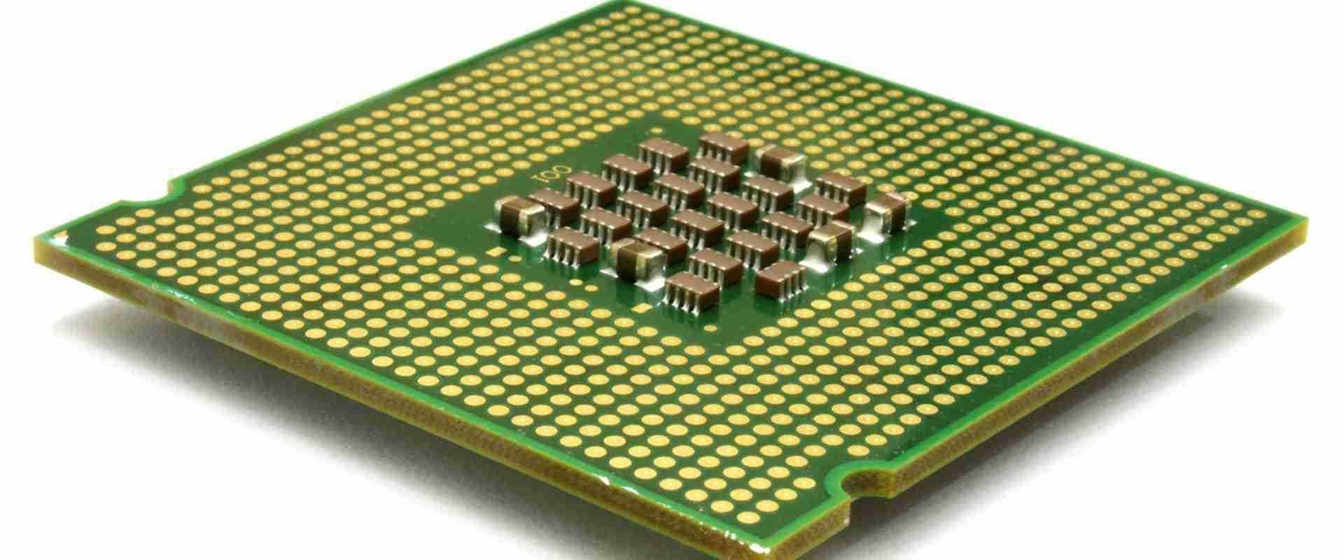 IC Substrate example showcasing high density interconnects
Ultra-High Density Interconnect (UHDI) PCBs: Pushing the Boundaries
The next frontier in PCB design and fabrication involves a convergence with component packaging technologies, specifically IC substrates. IC substrates are used to house semiconductor chips within integrated circuits. In advanced processors and digital/RF modules, chips are mounted onto an IC substrate, which provides the crucial interconnections between the electrical contacts on the semiconductor die and the PCB itself. Cutting-edge ICs are now achieving feature sizes comparable to those found in IC substrates. Consequently, the same advanced manufacturing processes are increasingly being employed to produce both IC substrates and ultra-high density interconnect (UHDI) PCBs.
The extremely fine feature sizes characteristic of UHDI PCBs are pushing the limits of manufacturing capabilities. Currently, large-scale UHDI production is primarily concentrated in regions like Taiwan. However, global UHDI manufacturing capacity is expanding due to substantial investments in advanced manufacturing technologies worldwide. The fabrication techniques for UHDI PCBs are predominantly additive. Traces and vias (vertical connections between layers) are formed through metal deposition processes, rather than the subtractive etching methods used in conventional PCB manufacturing. UHDI PCBs are poised to be the driving force behind the most advanced electronic systems, enabling operation at the highest data rates in applications such as high-speed computing and advanced communication networks. While the manufacturing processes differ significantly, the design process for UHDI PCBs remains remarkably similar to that of conventional PCBs, leveraging the same ECAD software and design principles.
Embarking on a New PCB Design Project
When initiating a new electronic product design, the printed circuit board design process typically involves several well-defined stages. Production-grade PCBs are designed using specialized ECAD software. ECAD software packages are CAD applications specifically tailored for circuit board design and layout, incorporating a wide range of utilities and features optimized for this purpose. ECAD software guides designers through a structured PCB design workflow, commencing with schematic capture (creating electrical diagrams) and culminating in the generation of manufacturing files ready for PCB fabrication. The fundamental PCB design process generally follows these key steps:
- Schematic Capture: Creating the electrical circuit diagram representing the intended functionality.
- Component Selection: Choosing appropriate electronic components based on circuit requirements and performance specifications.
- PCB Layout: Physically arranging components and routing electrical connections (traces) on the PCB within the ECAD software.
- Design Rule Checking (DRC): Verifying the PCB layout against predefined design rules and manufacturing constraints to ensure manufacturability and functionality.
- Gerber File Generation: Creating manufacturing files (Gerber files) that contain all the necessary information for PCB fabrication.
- PCB Fabrication: Manufacturing the bare PCB based on the generated Gerber files.
- PCB Assembly (PCBA): Soldering electronic components onto the fabricated PCB.
- Testing and Validation: Testing the assembled PCBA to verify its functionality and performance against design specifications.
To effectively navigate these stages of the PCB electronics board design process, utilizing robust design software equipped with an intuitive user interface and a comprehensive suite of PCB design features is essential.
Altium Designer: Your Comprehensive PCB Design Solution
The most effective ECAD software should be user-friendly, easy to learn, and encompass a complete set of design capabilities. Altium Designer stands out as a unified application that integrates all necessary tools within a single program. No external programs are needed to complete a design and prepare it for manufacturing.
 3D view of a PCB layout in Altium Designer
3D visualization of a completed PCB layout within Altium Designer.
Altium Designer’s unified design environment provides all the tools needed to design and manufacture high-quality printed circuit board assemblies. In contrast, other software programs often fragment design workflows across multiple separate applications with disparate interfaces, hindering productivity and potentially increasing software licensing costs. Altium Designer is consistently recognized for its ease of learning and user-friendliness, making it an excellent choice for both novice and experienced PCB designers.
Altium Designer, in conjunction with the Altium 365 cloud platform, brings unprecedented levels of integration to the electronics industry. By leveraging cloud-based collaboration and data management, Altium 365 enables designers to work remotely and achieve new levels of design efficiency.
This article has only touched upon the vast capabilities of Altium Designer and Altium 365. To explore the full potential, consider starting a free trial of Altium Designer + Altium 365 today.