
Electronic devices are the backbone of modern life. From life-saving medical equipment to the smartphones in our pockets, Printed Circuit Boards (PCBs) are at the heart of almost every electronic gadget. As technology advances, the demand for PCBs that are faster, smaller, and more complex continues to grow. The intricacies of PCB design and development are vast, but this guide offers a foundational understanding of the key aspects of Printed Circuit Board Design.
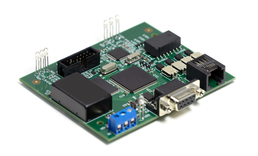 Picture of a standard printed circuit board
Understanding Printed Circuit Boards
Essentially, a printed circuit board is the foundation upon which electronic components are mounted and interconnected. It’s a rigid board constructed from a non-conductive material, featuring conductive pathways, known as traces, and larger conductive areas, called planes. These conductive elements, typically made of copper, are etched onto the board’s surface or embedded within multiple layers. Components are then soldered to metallic pads on the PCB, establishing electrical connections through the traces and planes. PCBs can range from single-layer boards to complex multi-layer structures, depending on the circuit’s complexity.
PCBs are manufactured using dielectric core materials, which are poor electrical conductors. This ensures efficient signal transmission within the circuitry. Layers of metal conductors and dielectric materials are stacked to create the desired board structure. The industry-standard dielectric material is FR-4, a flame-retardant composite of fiberglass cloth and epoxy resin. Copper is the most common metal used for traces and planes due to its excellent conductivity.
PCB Board Classifications
PCBs are classified into three classes – Class 1, Class 2, and Class 3 – based on their reliability and quality requirements. This classification is crucial in printed circuit board design as it dictates manufacturing standards and quality control.
Class 1 PCBs are general-purpose boards typically used in consumer electronics where functionality is primary and high reliability is not critical. Acceptable cosmetic imperfections are allowed as long as they don’t impact function.
Class 2 PCBs are used in applications where high reliability is important but not life-dependent. These boards are found in industrial controls, communication equipment, and business machines. They demand higher quality than Class 1, aiming to minimize failures and ensure extended operational life.
Class 3 PCBs represent the highest reliability standards in PCB manufacturing and design. These boards are mission-critical and must perform flawlessly in demanding environments. Failure of a Class 3 PCB could have severe consequences, including loss of life. Examples include PCBs used in aerospace, medical life support systems, and military applications.
Types of Printed Circuit Boards
PCBs can also be categorized by their physical structure and flexibility into rigid, flexible, and metal-core PCBs. Understanding these types is crucial for effective printed circuit board design.
Rigid PCBs are the most common type, built on a solid, inflexible substrate, typically FR-4. The layers are laminated together using heat and pressure. Rigid PCBs are cost-effective and suitable for a wide range of applications, from simple electronics to complex systems. Variations in rigid PCB materials allow for tailored performance characteristics.
Flexible PCBs, or flex PCBs, are constructed on a flexible substrate material, such as polyimide film. This allows the board to bend and conform to various shapes, making them ideal for applications where space is limited or where dynamic flexing is required. Flexible PCBs are commonly used in wearable technology, automotive electronics, and foldable devices.
Metal-core PCBs, also known as MCPCBs, are a specialized type of rigid PCB that incorporates a metal base material, typically aluminum. The metal core acts as a heat sink, efficiently dissipating heat away from heat-generating components. Metal-core PCBs are advantageous in high-power applications such as LED lighting, power supplies, and automotive systems where thermal management is critical for reliability.
Printed circuit boards are essential for organizing and supporting electronic components in virtually any device requiring controlled electromagnetism. The journey from concept to a finished PCB involves a complex design and manufacturing process.
The Printed Circuit Board Design Process
Before manufacturing, a PCB must undergo a rigorous design process. This is where printed circuit board design expertise comes into play. Computer-Aided Design (CAD) tools are indispensable for this process. PCB design is broadly divided into two key phases: schematic capture and PCB layout.
Library CAD Part Development
The initial step in printed circuit board design is creating a comprehensive library of CAD parts. This library contains all the necessary information for each component to be used in the design. Each component requires:
- Schematic Symbol: A graphical representation used in the schematic diagram.
- Simulation Model: Data for circuit simulation to verify electrical performance.
- PCB Footprint: The physical land pattern that defines how the component is mounted on the PCB.
- 3D Model: A 3D representation for visualization and mechanical integration checks.
Creating accurate and complete library parts is crucial for a smooth and error-free design process.
Schematic Capture and Circuit Simulation
Once the component libraries are established, the next stage is schematic capture. This involves creating a logical representation of the electronic circuit using schematic CAD tools. Designers place schematic symbols onto a virtual sheet and connect them using wires to define the circuit’s connectivity.
Simultaneously, circuit simulation is performed to validate the design’s electrical functionality. Simulation software, like SPICE, analyzes the circuit based on component models and predicts its behavior. This crucial step helps identify and rectify design flaws early in the process, saving time and resources.
After schematic capture and simulation are complete, the design data, including component connectivity (netlist), is transferred to the PCB layout tools.
PCB Layout Design
In the PCB layout phase, the physical realization of the circuit board takes place. The layout designer receives the netlist from the schematic and uses PCB CAD tools to arrange components and route the interconnections.
The process starts with defining the board outline. Then, component footprints are placed strategically within the board area. Optimal component placement considers factors like signal integrity, thermal management, and manufacturability.
Once components are placed, the next critical step is routing. This involves drawing conductive traces and planes to connect component pins according to the netlist. PCB CAD tools incorporate design rule checks (DRC) to ensure that routing adheres to industry standards and design specifications. DRC helps prevent shorts, insufficient clearances, and other layout errors.
After routing is completed, manufacturing files, such as Gerber files and drill files, are generated. These files contain all the necessary information for PCB fabrication and assembly.
The entire printed circuit board design process is iterative, involving schematic design, simulation, layout, and verification, culminating in the manufacturing-ready design files.
Steps in Making a Printed Circuit Board
While printed circuit board design provides the blueprint, manufacturing brings the design to life. The manufacturing process involves several detailed steps.
Schematic Creation
The initial step in the design workflow is schematic creation using CAD tools. This requires having well-defined library parts, including schematic symbols for components like resistors, capacitors, inductors, connectors, and integrated circuits (ICs).
Designers arrange these symbols on schematic sheets and then use virtual wires to connect component pins, representing electrical connections. These connections are called nets and can represent single signals or groups of signals, such as data buses or memory interfaces. The schematic should be clear, legible, and logically organized for easy understanding and review.
Circuit Simulation
After the schematic is drawn, circuit simulation is crucial to verify the circuit’s intended functionality. Simulation software, often based on SPICE, allows engineers to test the circuit design virtually before physical prototyping. This process helps identify potential design flaws, optimize component values, and ensure the circuit meets performance requirements. Circuit simulation saves time and cost by preventing costly rework later in the design cycle.
CAD Tool Setup: Design Rules and Grids
Setting up the CAD environment correctly is essential for efficient and error-free printed circuit board design. This involves defining design rules and constraints that govern the layout process. Design rules specify clearances between traces, trace widths, via sizes, and other parameters to ensure manufacturability and signal integrity.
Design grids are also established to aid in precise component placement and routing. Grids help maintain alignment and spacing, contributing to a neat and orderly layout.
 Schematic example using OrCAD Capture
An example of a schematic created using OrCAD Capture
Component Placement
With the design database configured and connectivity data imported from the schematic, component placement is the next critical step in PCB layout. Designers place component footprints within the defined board outline. CAD tools display “ratsnest” lines, indicating the connections between component pins based on the netlist.
Effective component placement is a skill honed with experience. It involves considering factors like:
- Connectivity: Minimizing trace lengths and crossings.
- Performance: Placing critical components for optimal signal integrity and thermal management.
- Manufacturability: Ensuring components are placed for efficient assembly and soldering.
- Physical Constraints: Accommodating connectors, mounting hardware, and enclosure requirements.
PCB Routing
Once components are placed, PCB routing connects the component pins using traces and planes. This process converts the ratsnest lines into physical copper pathways. CAD tools offer various routing features, including manual routing, auto-routing, and semi-auto routing.
Careful routing is essential for signal integrity and overall PCB performance. Designers must consider:
- Trace Length: Controlling trace lengths for critical signals to minimize signal delay and reflections.
- Trace Impedance: Maintaining controlled impedance for high-speed signals.
- Signal Isolation: Separating sensitive signals from noisy signals to prevent crosstalk.
- Routing Angles: Using appropriate routing angles to minimize signal reflections.
Ensuring a Clear Return Current Path
Power and ground planes are crucial aspects of printed circuit board design. They provide power distribution and serve as return current paths for signals. Solid, uninterrupted power and ground planes are ideal for minimizing noise and ensuring signal integrity.
However, planes are often interrupted by vias, component pins, and cutouts. Designers must carefully manage plane design to maintain clear return current paths. Discontinuities in return paths can lead to signal reflections, increased EMI (Electromagnetic Interference), and degraded signal performance.
Final Design Checks and Manufacturing Files
After component placement, routing, and plane design are complete, final design checks are performed. This includes running DRC to verify design rule compliance and performing signal integrity analysis to ensure signal performance.
Silkscreen layers are added to the PCB to provide component identification, part numbers, logos, and other markings for assembly and traceability. Manufacturing files, including Gerber files, drill files, and netlists, are generated. These files are sent to the PCB fabricator and assembly house to manufacture and assemble the board. Cost estimations are also typically generated from the design data.
**
Here is an example of a printed circuit board created with OrCAD PCB Designer
PCB Fabrication and Assembly
The final step is PCB fabrication and assembly. Fabrication involves manufacturing the bare PCB based on the generated design files. This includes:
- Imaging and Etching: Transferring the circuit patterns onto copper layers and etching away unwanted copper.
- Layer Lamination: Bonding multiple layers together to form the multi-layer PCB.
- Drilling: Creating holes for vias and component pins.
- Plating: Plating vias and surface pads for solderability and conductivity.
- Surface Finish: Applying a protective surface finish, such as solder mask and surface finish plating.
Once fabrication is complete, the bare PCBs are sent to the assembly facility. Assembly involves:
- Component Placement: Automatically placing components onto the PCB.
- Soldering: Soldering components to the PCB using reflow soldering or wave soldering techniques.
- Inspection and Testing: Inspecting and testing the assembled PCBs to ensure functionality and quality.
After successful testing, the assembled PCBs are ready for shipment.
Leveraging PCB Tools for Superior Design
The processes of PCB fabrication and assembly demand precision and adherence to stringent specifications. To ensure that manufactured PCBs meet performance requirements, accurate and comprehensive design data is crucial.
Printed circuit board design tools must provide the capabilities and features needed to handle complex designs. This includes:
- Advanced Routing Features: Tools for routing high-speed signals, differential pairs, and complex geometries.
- Design Rule Management: Flexible and customizable design rule setup for various design constraints.
- Simulation and Analysis: Integrated simulation tools for circuit, signal integrity, and thermal analysis.
- Comprehensive Component Libraries: Extensive libraries of pre-built component models and footprints.
For high-quality printed circuit board design, consider utilizing professional-grade CAD tools like the Cadence PCB design system. Cadence offers a comprehensive suite of tools for schematic capture, PCB layout, simulation, and analysis, catering to the demands of modern electronic design.
Leading electronics companies worldwide rely on Cadence solutions to optimize power, space, and energy efficiency across diverse market applications. To explore Cadence’s innovative solutions further, contact our team of experts or subscribe to our YouTube channel for valuable insights and tutorials.